MW5IC970NBR1 Freescale Semiconductor, MW5IC970NBR1 Datasheet

IC PWR AMP RF 28V 70W TO-272-16

MW5IC970NBR1

Manufacturer Part Number
MW5IC970NBR1
Description
IC PWR AMP RF 28V 70W TO-272-16
Manufacturer
Freescale Semiconductor
Type
Power Amplifierr
Datasheets

Specifications of MW5IC970NBR1

Current - Supply
80mA
Frequency
800MHz ~ 900MHz
Gain
30dB
Package / Case
TO-272-16
Rf Type
General Purpose
Voltage - Supply
28V
Number Of Channels
1
Frequency (max)
900MHz
Power Supply Requirement
Single
Single Supply Voltage (typ)
28V
Dual Supply Voltage (min)
Not RequiredV
Dual Supply Voltage (typ)
Not RequiredV
Dual Supply Voltage (max)
Not RequiredV
Pin Count
16
Mounting
Surface Mount
Lead Free Status / RoHS Status
Lead free / RoHS Compliant
Noise Figure
-
P1db
-
Test Frequency
-
Lead Free Status / Rohs Status
Compliant

Available stocks

Company
Part Number
Manufacturer
Quantity
Price
Part Number:
MW5IC970NBR1
Manufacturer:
ZCOMM
Quantity:
1 400
Part Number:
MW5IC970NBR1
Manufacturer:
FREESCALE
Quantity:
20 000
© Freescale Semiconductor, Inc., 2006. All rights reserved.
RF Device Data
Freescale Semiconductor
Technical Data
RF LDMOS Wideband 2 - Stage
Power Amplifiers
cies from 132 MHz to 960 MHz. The high gain and broadband performance of
this device make it ideal for large - signal, common - source amplifier applica-
tions in 28 volt base station equipment. The device has a 2 - stage design with
off - chip matching for the input, interstage and output networks to cover the
desired frequency band.
• Typical Performance: 800 MHz, 28 Volts, I
• Capable of Handling 10:1 VSWR, @ 28 Vdc, 850 MHz, 70 Watts CW
Features
• Characterized with Series Equivalent Large - Signal Impedance Parameters
• Integrated Quiescent Current Temperature Compensation
• On - Chip Current Mirror g
• Integrated ESD Protection
• 200°C Capable Plastic Package
• RoHS Compliant
• In Tape and Reel. R1 Suffix = 500 Units per 44 mm, 13 inch Reel.
1. Refer to AN1987, Quiescent Current Control for the RF Integrated Circuit Device Family. Go to http://www.freescale.com/rf.
Designed for broadband commercial and industrial applications with frequen-
I
Output Power
with Enable/Disable Function
DQ2
Select Documentation/Application Notes - AN1987.
V
V
V
V
Power Gain — 30 dB
Drain Efficiency — 48%
RG2
RG1
D1
D1
= 650 mA, P
/RF
/RF
/V
/V
V
RF
RF
V
RD1
RD2
GS2
GS1
out1
out1
in1
in2
out
Figure 1. Functional Block Diagram
= 70 Watts PEP
m
Reference FET for Self Biasing Application
Temperature Compensation
Quiescent Current
DQ1
= 80 mA,
V
D2
/RF
out2
(1)
Document Number: MW5IC970NBR1
Note: Exposed backside flag is source
2 - STAGE POWER AMPLIFIERS
V
V
V
V
MW5IC970NBR1
RG1
RG2
D1
D1
800 - 900 MHz, 70 W, 28 V
Figure 2. Pin Connections
/RF
RF LDMOS WIDEBAND
/RF
/V
/V
RF
RF
V
GND
GND
V
GND
terminal for transistors.
RD2
GS2
GS1
RD1
out1
out1
in1
in2
TO - 272 WB - 16
CASE 1329 - 09
PLASTIC
10
11
1
2
3
4
5
6
7
8
9
(Top View)
MW5IC970NBR1
Rev. 1, 5/2006
16
15
14
13
12
GND
NC
V
RF
NC
GND
D2/
out2
1

Related parts for MW5IC970NBR1

MW5IC970NBR1 Summary of contents

Page 1

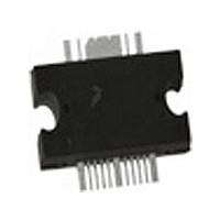
... Select Documentation/Application Notes - AN1987. © Freescale Semiconductor, Inc., 2006. All rights reserved. RF Device Data Freescale Semiconductor = 80 mA, DQ1 (1) V /RF D2 out2 Document Number: MW5IC970NBR1 Rev. 1, 5/2006 MW5IC970NBR1 800 - 900 MHz LDMOS WIDEBAND 2 - STAGE POWER AMPLIFIERS CASE 1329 - 272 PLASTIC GND 1 GND ...

Page 2

... Gain Flatness in 30 MHz Instantaneous Bandwidth @ out Delay @ Including Output Matching out Part - to - Part Phase Variation @ out 1. Refer to AN1955, Thermal Measurement Methodology of RF Power Amplifiers http://www.freescale.com/rf. Select Documentation/Application Notes - AN1955. MW5IC970NBR1 2 Stage 1, 28 Vdc Stage 2, 28 Vdc 650 mA DQ Stage 1, 28 Vdc Stage 2, 28 Vdc, I ...

Page 3

... Z4 0.950″ x 0.040″ Microstrip Z5 0.131″ x 0.233″ Microstrip Z6 0.797″ x 0.050″ Microstrip Figure 3. MW5IC970NBR1 Test Circuit Schematic Table 6. MW5IC970NBR1 Test Circuit Component Designations and Values Part C1, C10, C11 3.9 pF Chip Capacitor Chip Capacitor C3, C8, C14, C15, C17 39 pF Chip Capacitors C4 μ ...

Page 4

... Figure 4. MW5IC970NBR1 Test Circuit Component Layout MW5IC970NBR1 C18 C17 C16 C15 MW5IC970 C4 Rev C11 C13 C7 C10 C12 C14 RF Device Data Freescale Semiconductor ...

Page 5

... Vdc = 80 mA 650 mA DQ2 3rd Order 5th Order 7th Order 10 100 P , OUTPUT POWER (WATTS) PEP out versus Output Power = 80 mA −30_C DQ1 25_C −30_C 85_C G ps 85_C PAE 1 10 100 P , OUTPUT POWER (WATTS) CW out MW5IC970NBR1 300 1000 5 ...

Page 6

... MW5IC970NBR1 6 TYPICAL CHARACTERISTICS I DQ1 I DQ2 f = 870 MHz 28 100 P , OUTPUT POWER (WATTS) CW out Figure 10. Power Gain versus Output Power = 650 120 140 RF Device Data Freescale Semiconductor ...

Page 7

... RF Device Data Freescale Semiconductor NOTES MW5IC970NBR1 7 ...

Page 8

... MW5IC970NBR1 8 NOTES RF Device Data Freescale Semiconductor ...

Page 9

... RF Device Data Freescale Semiconductor PACKAGE DIMENSIONS MW5IC970NBR1 9 ...

Page 10

... MW5IC970NBR1 10 RF Device Data Freescale Semiconductor ...

Page 11

... RF Device Data Freescale Semiconductor MW5IC970NBR1 11 ...

Page 12

... Denver, Colorado 80217 1 - 800- 441- 2447 or 303 - 675- 2140 Fax: 303 - 675- 2150 LDCForFreescaleSemiconductor@hibbertgroup.com MW5IC970NBR1 Document Number: MW5IC970NBR1 Rev. 1, 5/2006 12 Information in this document is provided solely to enable system and software implementers to use Freescale Semiconductor products. There are no express or implied copyright licenses granted hereunder to design or fabricate any integrated circuits or integrated circuits based on the information in this document ...

Related keywords