MW5IC970NBR1 Freescale Semiconductor, MW5IC970NBR1 Datasheet
MW5IC970NBR1
Specifications of MW5IC970NBR1
Available stocks


Related parts for MW5IC970NBR1

MW5IC970NBR1 Summary of contents
Page 1
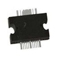
... CASE 1329A-04 TO-272 WB-16 GULL PLASTIC MW5IC970GNBR1 GND 1 GND RD2 RG2 GS2 RG1 GS1 5 RF in1 V D2/ GND out2 V 7 RD1 V / out1 V / out1 in2 12 GND 11 GND (Top View) Note: Exposed backside flag is source terminal for transistors. Figure 2. Pin Connections MW5IC970NBR1 MW5IC970GNBR1 1 ...
Page 2
... Gain Flatness in 30 MHz Instantaneous Bandwidth @ out Delay @ Including Output Matching out Part-to-Part Phase Variation @ out 1. Refer to AN1955, Thermal Measurement Methodology of RF Power Amplifiers http://www.freescale.com/rf. Select Documentation/Application Notes - AN1955. MW5IC970NBR1 MW5IC970GNBR1 2 Stage 1, 28 Vdc Stage 2, 28 Vdc 650 mA DQ Stage 1, 28 Vdc Stage 2, 28 Vdc, I ...
Page 3
... Z4 0.950″ x 0.040″ Microstrip Z5 0.131″ x 0.233″ Microstrip Z6 0.797″ x 0.050″ Microstrip Figure 3. MW5IC970NBR1(GNBR1) Test Circuit Schematic Table 6. MW5IC970NBR1(GNBR1) Test Circuit Component Designations and Values Part C1, C10, C11 3.9 pF Chip Capacitors Chip Capacitor C3, C8, C14, C15, C17 39 pF Chip Capacitors 10 μ ...
Page 4
... Figure 4. MW5IC970NBR1(GNBR1) Test Circuit Component Layout MW5IC970NBR1 MW5IC970GNBR1 C18 C17 C16 C15 MW5IC970 C4 Rev C11 C13 C7 C10 C12 C14 RF Device Data Freescale Semiconductor ...
Page 5
... Vdc = 80 mA 650 mA DQ2 3rd Order 5th Order 7th Order 10 100 P , OUTPUT POWER (WATTS) PEP out versus Output Power - DQ1 25_C -30 _C 85_C G ps 85_C PAE 1 10 100 P , OUTPUT POWER (WATTS) CW out MW5IC970NBR1 MW5IC970GNBR1 300 1000 5 ...
Page 6
... MW5IC970NBR1 MW5IC970GNBR1 6 TYPICAL CHARACTERISTICS I DQ1 I DQ2 f = 870 MHz 28 100 P , OUTPUT POWER (WATTS) CW out Figure 10. Power Gain versus Output Power = 650 120 140 RF Device Data Freescale Semiconductor ...
Page 7
... RF Device Data Freescale Semiconductor PACKAGE DIMENSIONS MW5IC970NBR1 MW5IC970GNBR1 7 ...
Page 8
... MW5IC970NBR1 MW5IC970GNBR1 8 RF Device Data Freescale Semiconductor ...
Page 9
... RF Device Data Freescale Semiconductor MW5IC970NBR1 MW5IC970GNBR1 9 ...
Page 10
... MW5IC970NBR1 MW5IC970GNBR1 10 RF Device Data Freescale Semiconductor ...
Page 11
... RF Device Data Freescale Semiconductor MW5IC970NBR1 MW5IC970GNBR1 11 ...
Page 12
... MW5IC970NBR1 MW5IC970GNBR1 12 RF Device Data Freescale Semiconductor ...
Page 13
... EB212: Using Data Sheet Impedances for RF LDMOS Devices The following table summarizes revisions to this document. Revision Date • Document Number changed from MW5IC970NBR1 to MW5IC970N with the addition of the 2 Apr. 2008 MW5IC970GNBR1 part number. Revision history sequencing maintained from first release of data sheet • ...
Page 14
... For Literature Requests Only: Freescale Semiconductor Literature Distribution Center 1-800-441-2447 or +1-303-675-2140 Fax: +1-303-675-2150 LDCForFreescaleSemiconductor@hibbertgroup.com MW5IC970NBR1 MW5IC970GNBR1 Document Number: MW5IC970N Rev. 3, 1/2010 14 Information in this document is provided solely to enable system and software implementers to use Freescale Semiconductor products. There are no express or implied copyright licenses granted hereunder to design or fabricate any integrated circuits or integrated circuits based on the information in this document ...