TWR-MCF51JE Freescale Semiconductor, TWR-MCF51JE Datasheet - Page 21
TWR-MCF51JE
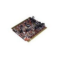
Manufacturer Part Number
TWR-MCF51JE
Description
TOWER SYSTEM BOARD MCF51JE
Manufacturer
Freescale Semiconductor
Series
ColdFire®, Flexis™r
Type
MCUr
Specifications of TWR-MCF51JE
Contents
Board
Data Bus Width
32 bit
Interface Type
RS-232, RS-485, Ethernet, CAN, USB
Silicon Manufacturer
Freescale
Core Architecture
Coldfire
Core Sub-architecture
Coldfire V1
Silicon Core Number
MCF51J
Silicon Family Name
Flexis - MCF51JE
Rohs Compliant
Yes
For Use With/related Products
Freescale Tower System, MCF51JE
Lead Free Status / RoHS Status
Lead free / RoHS Compliant


Freescale Semiconductor
1
2
3
4
5
6
7
Num Symbol
19
20
21
22
23
24
Typical values are measured at 25°C. Characterized, not tested
As the supply voltage rises, the LVD circuit will hold the MCU in reset until the supply has risen above V
Measured with V
All functional non-supply pins are internally clamped to V
Input must be current limited to the value specified. To determine the value of the required current-limiting resistor,
calculate resistance values for positive and negative clamp voltages, then use the larger of the two values.
Power supply must maintain regulation within operating V
conditions. If positive injection current (V
result in external power supply going out of regulation. Ensure external V
injection current. This will be the greatest risk when the MCU is not consuming power. Examples are: if no system clock
is present, or if clock rate is very low (which would reduce overall power consumption).
Maximum is highest voltage that POR is guaranteed.
V
V
V
V
LVDH
V
V
LVWH
LVWL
LVDL
hys
BG
8
Low-voltage
detection
threshold —
high range
Low-voltage
detection
threshold —
low range
Low-voltage
warning
threshold —
high range
Low-voltage
warning
threshold —
low range
Low-voltage inhibit
reset/recoverhysteresis
Bandgap Voltage Reference
In
= V
DD
.
8
8
Characteristic
8
Table 9. DC Characteristics (Continued)
Preliminary — Subject to Change
V
V
V
V
V
V
V
V
DD
DD
DD
DD
DD
DD
DD
DD
In
> V
9
falling
rising
falling
rising
falling
rising
falling
rising
DD
10
) is greater than I
DD
SS
Condition
range during instantaneous and operating maximum current
and V
—
—
—
—
—
—
—
—
—
—
DD
DD
, the injection current may flow out of V
.
DD
1.145
2.11
2.16
1.80
1.86
2.36
2.36
2.11
2.16
Min
load will shunt current greater than maximum
—
Typ
2.16
2.21
1.82
1.90
2.46
2.46
2.16
2.21
1.17
50
Preliminary Electrical Characteristics
1
1.195
Max
2.22
2.27
1.91
1.99
2.56
2.56
2.22
2.27
—
LVDL
Unit
mV
V
V
V
V
V
V
V
V
V
DD
.
and could
C
P
P
P
P
P
P
P
P
C
P
1-2
Related parts for TWR-MCF51JE
Image
Part Number
Description
Manufacturer
Datasheet
Request
R

Part Number:
Description:
Power Management IC Development Tools Low-volt 3-phase MC
Manufacturer:
Freescale Semiconductor
Datasheet:
Part Number:
Description:
K53N512CMD100 TWR Module
Manufacturer:
Freescale Semiconductor
Datasheet:
Part Number:
Description:
TWR-K53N512 Dev Kit
Manufacturer:
Freescale Semiconductor
Datasheet:

Part Number:
Description:
CONV DC/DC TRI OUT 5,15,-15V
Manufacturer:
Murata Power Solutions Inc
Datasheet:

Part Number:
Description:
CONV DC/DC TRI OUT 5,12,-12V
Manufacturer:
Murata Power Solutions Inc
Datasheet:

Part Number:
Description:
CONV DC/DC TRI OUT 5,15,-15V
Manufacturer:
Murata Power Solutions Inc
Datasheet:

Part Number:
Description:
LCD MODULE FOR TWR SYSTEM
Manufacturer:
Freescale Semiconductor
Datasheet:

Part Number:
Description:
DC/DC TH 11W 5-5/12V Triple A
Manufacturer:
Murata Power Solutions Inc
Datasheet:


Part Number:
Description:
TOWER SYSTEM PROTO
Manufacturer:
Freescale Semiconductor
Datasheet:

Part Number:
Description:
TOWER ELEVATOR BOARDS HARDWARE
Manufacturer:
Freescale Semiconductor
Datasheet:

Part Number:
Description:
TOWER SERIAL I/O HARDWARE
Manufacturer:
Freescale Semiconductor
Datasheet:

Part Number:
Description:
TOWER SYSTEM BOARD MPC5125
Manufacturer:
Freescale Semiconductor
Datasheet: