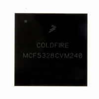
MCF5328CVM240 Freescale Semiconductor, MCF5328CVM240 Datasheet - Page 6

MCF5328CVM240
Manufacturer Part Number
MCF5328CVM240
Description
IC MCU 32BIT 240MHZ 256-MAPBGA
Manufacturer
Freescale Semiconductor
Series
MCF532xr
Datasheet
1.MCF5328CVM240J.pdf
(50 pages)
Specifications of MCF5328CVM240
Core Processor
Coldfire V3
Core Size
32-Bit
Speed
240MHz
Connectivity
EBI/EMI, Ethernet, I²C, SPI, SSI, UART/USART, USB, USB OTG
Peripherals
DMA, LCD, PWM, WDT
Number Of I /o
94
Program Memory Type
ROMless
Ram Size
32K x 8
Voltage - Supply (vcc/vdd)
1.4 V ~ 3.6 V
Oscillator Type
External
Operating Temperature
-40°C ~ 85°C
Package / Case
256-MAPBGA
Program Memory Size
16KB
Cpu Speed
240MHz
Embedded Interface Type
CAN, I2C, MAC, Ethernet, QSPI, UART
Rohs Compliant
Yes
Family Name
MPC5xxx
Device Core
ColdFire
Device Core Size
32b
Frequency (max)
240MHz
Instruction Set Architecture
RISC
Supply Voltage 1 (typ)
1.8/2.5/3.3V
Operating Supply Voltage (max)
1.6/1.95/2.75/3.6V
Operating Supply Voltage (min)
1.4/1.7/2.25/3V
Operating Temp Range
-40C to 85C
Operating Temperature Classification
Industrial
Mounting
Surface Mount
Pin Count
256
Package Type
MA-BGA
Lead Free Status / RoHS Status
Lead free / RoHS Compliant
Eeprom Size
-
Program Memory Size
-
Data Converters
-
Lead Free Status / Rohs Status
Compliant
Available stocks
Company
Part Number
Manufacturer
Quantity
Price
Company:
Part Number:
MCF5328CVM240
Manufacturer:
FREESCAL
Quantity:
717
Company:
Part Number:
MCF5328CVM240
Manufacturer:
Freescale Semiconductor
Quantity:
10 000
Part Number:
MCF5328CVM240
Manufacturer:
FREESCALE
Quantity:
20 000
Company:
Part Number:
MCF5328CVM240J
Manufacturer:
Freescale Semiconductor
Quantity:
10 000
Pin Assignments and Reset States
high current in the internal ESD protection diodes. The rise times on the power supplies should be slower than 500 us to avoid
turning on the internal ESD protection clamp diodes.
3.3.2
If IV
There is no limit on how long after IV
not lag EV
ESD protection diodes. There are no requirements for the fall times of the power supplies.
The recommended power down sequence is as follows:
4
4.1
The following table lists all the MCF532x pins grouped by function. The Dir column is the direction for the primary function
of the pin only. Refer to
MCF532x signals, consult the MCF5329 Reference Manual (MCF5329RM).
6
Signal Name
1.
2.
DD
EXTAL32K
XTAL32K
RSTOUT
RESET
FB_CLK
/PLLV
EXTAL
XTAL
Drop IV
Drop EV
DD
Pin Assignments and Reset States
Signal Multiplexing
2
, SDV
2
Power Down Sequence
DD
DD
are powered down first, sense circuits in the I/O pads cause all output drivers to be in a high impedance state.
In this table and throughout this document, a single signal within a group is designated
without square brackets (i.e., A23), while designations for multiple signals within a group
use brackets (i.e., A[23:21]) and is meant to include all signals within the two bracketed
numbers when these numbers are separated by a colon.
The primary functionality of a pin is not necessarily its default functionality. Pins that are
muxed with GPIO default to their GPIO functionality.
DD
DD
/PLLV
/SDV
, or PLLV
Section 7, “Package
GPIO
DD
DD
—
—
—
—
—
—
—
supplies.
to 0 V.
Table 3. MCF5327/8/9 Signal Information and Muxing
DD
MCF532x ColdFire
going low by more than 0.4 V during power down or there is undesired high current in the
DD
Alternate 1
and PLLV
—
—
—
—
—
—
—
Information,”
DD
®
Alternate 2
power down before EV
Microprocessor Data Sheet, Rev. 5
NOTE
NOTE
for package diagrams. For a more detailed discussion of the
—
—
—
—
—
—
—
Reset
Clock
O
O
O
O
I
I
I
SDVDD
EVDD
EVDD
EVDD
EVDD
EVDD
EVDD
DD
or SDV
MAPBGA
MCF5327
M11
N11
P14
K14
196
J11
L14
L1
DD
must power down. IV
MAPBGA
MCF5328
Freescale Semiconductor
N15
P14
P16
N16
P13
R13
256
T2
MCF53281
MCF5329
MAPBGA
DD
N15
P14
P16
N16
P13
R13
256
T2
should


