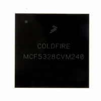
MCF5328CVM240 Freescale Semiconductor, MCF5328CVM240 Datasheet - Page 26

MCF5328CVM240
Manufacturer Part Number
MCF5328CVM240
Description
IC MCU 32BIT 240MHZ 256-MAPBGA
Manufacturer
Freescale Semiconductor
Series
MCF532xr
Datasheet
1.MCF5328CVM240J.pdf
(50 pages)
Specifications of MCF5328CVM240
Core Processor
Coldfire V3
Core Size
32-Bit
Speed
240MHz
Connectivity
EBI/EMI, Ethernet, I²C, SPI, SSI, UART/USART, USB, USB OTG
Peripherals
DMA, LCD, PWM, WDT
Number Of I /o
94
Program Memory Type
ROMless
Ram Size
32K x 8
Voltage - Supply (vcc/vdd)
1.4 V ~ 3.6 V
Oscillator Type
External
Operating Temperature
-40°C ~ 85°C
Package / Case
256-MAPBGA
Program Memory Size
16KB
Cpu Speed
240MHz
Embedded Interface Type
CAN, I2C, MAC, Ethernet, QSPI, UART
Rohs Compliant
Yes
Family Name
MPC5xxx
Device Core
ColdFire
Device Core Size
32b
Frequency (max)
240MHz
Instruction Set Architecture
RISC
Supply Voltage 1 (typ)
1.8/2.5/3.3V
Operating Supply Voltage (max)
1.6/1.95/2.75/3.6V
Operating Supply Voltage (min)
1.4/1.7/2.25/3V
Operating Temp Range
-40C to 85C
Operating Temperature Classification
Industrial
Mounting
Surface Mount
Pin Count
256
Package Type
MA-BGA
Lead Free Status / RoHS Status
Lead free / RoHS Compliant
Eeprom Size
-
Program Memory Size
-
Data Converters
-
Lead Free Status / Rohs Status
Compliant
Available stocks
Company
Part Number
Manufacturer
Quantity
Price
Company:
Part Number:
MCF5328CVM240
Manufacturer:
FREESCAL
Quantity:
717
Company:
Part Number:
MCF5328CVM240
Manufacturer:
Freescale Semiconductor
Quantity:
10 000
Part Number:
MCF5328CVM240
Manufacturer:
FREESCALE
Quantity:
20 000
Company:
Part Number:
MCF5328CVM240J
Manufacturer:
Freescale Semiconductor
Quantity:
10 000
Electrical Characteristics
26
1
2
3
4
5
6
7
8
DD10
DD11 DQS falling edge from SDCLK rising (output hold time)
DD12 DQS input read preamble width
DD13 DQS input read postamble width
DD14 DQS output write preamble width
DD15 DQS output write postamble width
Num
DD8
DD9
SD_CLK is one SDRAM clock in (ns).
Pulse width high plus pulse width low cannot exceed min and max clock period.
Command output valid should be 1/2 the memory bus clock (SD_CLK) plus some minor adjustments for process, temperature,
and voltage variations.
This specification relates to the required input setup time of today’s DDR memories. The processor’s output setup should be
larger than the input setup of the DDR memories. If it is not larger, the input setup on the memory is in violation.
MEM_DATA[31:24] is relative to MEM_DQS[3], MEM_DATA[23:16] is relative to MEM_DQS[2], MEM_DATA[15:8] is relative to
MEM_DQS[1], and MEM_[7:0] is relative MEM_DQS[0].
The first data beat is valid before the first rising edge of DQS and after the DQS write preamble. The remaining data beats are
valid for each subsequent DQS edge.
This specification relates to the required hold time of today’s DDR memories. MEM_DATA[31:24] is relative to MEM_DQS[3],
MEM_DATA[23:16] is relative to MEM_DQS[2], MEM_DATA[15:8] is relative to MEM_DQS[1], and MEM_[7:0] is relative
MEM_DQS[0].
Data input skew is derived from each DQS clock edge. It begins with a DQS transition and ends when the last data line
becomes valid. This input skew must include DDR memory output skew and system level board skew (due to routing or other
factors).
Data input hold is derived from each DQS clock edge. It begins with a DQS transition and ends when the first data line
becomes invalid.
Data and Data Mask Output Hold (DQS-->DQ) Relative to
DQS (DDR Write Mode)
Input Data Skew Relative to DQS (Input Setup)
Input Data Hold Relative to DQS
Characteristic
6
MCF532x ColdFire
Table 11. DDR Timing Specifications (continued)
8
®
Microprocessor Data Sheet, Rev. 5
7
t
t
t
Symbol
DQLSDCH
t
t
DQWPRE
DQRPRE
DQWPST
DQRPST
t
t
DQDMI
t
DVDQ
DIDQ
0.25 × SD_CLK
+ 0.5ns
0.25
Min
1.0
0.5
0.9
0.4
0.4
—
Freescale Semiconductor
Max
1.1
0.6
0.6
—
—
—
1
SD_CLK
SD_CLK
SD_CLK
SD_CLK
Unit
ns
ns
ns
ns


