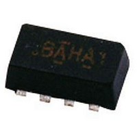
SI5499DC-T1-GE3 Vishay, SI5499DC-T1-GE3 Datasheet - Page 5

SI5499DC-T1-GE3
Manufacturer Part Number
SI5499DC-T1-GE3
Description
MOSFET P-CH D-S 1.5V 1206-8
Manufacturer
Vishay
Series
TrenchFET®r
Datasheet
1.SI5499DC-T1-GE3.pdf
(8 pages)
Specifications of SI5499DC-T1-GE3
Fet Type
MOSFET P-Channel, Metal Oxide
Fet Feature
Logic Level Gate
Rds On (max) @ Id, Vgs
36 mOhm @ 5.1A, 4.5V
Drain To Source Voltage (vdss)
8V
Current - Continuous Drain (id) @ 25° C
6A
Vgs(th) (max) @ Id
800mV @ 250µA
Gate Charge (qg) @ Vgs
35nC @ 8V
Input Capacitance (ciss) @ Vds
1290pF @ 4V
Power - Max
6.2W
Mounting Type
Surface Mount
Package / Case
1206-8 ChipFET™
Transistor Polarity
P Channel
Continuous Drain Current Id
-6A
Drain Source Voltage Vds
-8V
On Resistance Rds(on)
77mohm
Rds(on) Test Voltage Vgs
5V
Threshold Voltage Vgs Typ
-550mV
Lead Free Status / RoHS Status
Lead free / RoHS Compliant
Other names
SI5499DC-T1-GE3TR
TYPICAL CHARACTERISTICS 25 °C, unless otherwise noted
Document Number: 73321
S-83054-Rev. C, 29-Dec-08
0.7
0.6
0.5
0.4
0.3
0.2
40
10
1
- 50
0.0
- 25
Source-Drain Diode Forward Voltage
0.2
V
SD
0
0.4
- Source-to-Drain Voltage (V)
Threshold Voltage
T
J
25
- Temperature (°C)
T
J
0.6
= 150 °C
50
0.8
I
D
75
= 250 µA
0.01
100
1.0
0.1
T
100
10
0.01
J
1
= 25 °C
Safe Operating Area, Junction-to-Ambient
* V
1.2
125
GS
> minimum V
Limited by R
150
V
1.4
DS
-
0.1
Drain-to-Source Voltage (V )
Single Pulse
T
A
GS
= 25 °C
DS(on)
at which R
*
DS(on)
1
0.10
0.08
0.06
0.04
0.02
50
40
30
20
10
0
0.001
0
is specified
On-Resistance vs. Gate-to-Source Voltage
Single Pulse Power, Junction-to-Ambient
0.01
T
A
= 25 °C
1
V
10 ms
1 ms
100 ms
1 s
10 s
DC
10
GS
- Gate-to-Source Voltage (V)
0.1
2
Time (s)
1
Vishay Siliconix
T
A
3
= 125 °C
Si5499DC
10
www.vishay.com
I
D
4
100
= 5.1 A
1000
5
5


