ALD110900ASAL Advanced Linear Devices Inc, ALD110900ASAL Datasheet
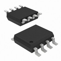
MOSFET N-CH 10.6V DUAL 8SOIC

ALD110900ASAL

Manufacturer Part Number
ALD110900ASAL
Description
MOSFET N-CH 10.6V DUAL 8SOIC
Manufacturer
Advanced Linear Devices Inc
Series
THRESHOLD™, EPAD®r
Datasheet

Specifications of ALD110900ASAL

Package / Case
8-SOIC (0.154", 3.90mm Width)
Fet Type
2 N-Channel (Dual)
Fet Feature
Standard
Drain To Source Voltage (vdss)
10.6V
Vgs(th) (max) @ Id
10mV @ 1µA
Power - Max
500mW
Mounting Type
Surface Mount
Minimum Operating Temperature
0 C
Configuration
Dual
Transistor Polarity
N-Channel
Resistance Drain-source Rds (on)
500 Ohm (Typ) @ 4 V
Forward Transconductance Gfs (max / Min)
0.0014 S
Drain-source Breakdown Voltage
10.6 V
Gate-source Breakdown Voltage
10.6 V
Continuous Drain Current
12 mA
Power Dissipation
500 mW
Maximum Operating Temperature
+ 70 C
Mounting Style
SMD/SMT
Lead Free Status / RoHS Status
Lead free / RoHS Compliant
Gate Charge (qg) @ Vgs
-
Current - Continuous Drain (id) @ 25° C
-
Rds On (max) @ Id, Vgs
-
Lead Free Status / Rohs Status
Lead free / RoHS Compliant
Other names
1014-1031
ORDERING INFORMATION
GENERAL DESCRIPTION
ALD110800A/ALD110800/ALD110900A/ALD110900 are monolithic quad/
dual N-Channel MOSFETs matched at the factory using ALD’s proven
EPAD CMOS technology. These devices are members of the EPAD
Matched Pair MOSFET Family.
Intended for low voltage, small signal applications, the ALD110800/
ALD110900 features zero threshold voltage, which reduces or eliminates
input to output voltage level shift, including circuits where the signal is
referenced to GND or V+. This feature greatly reduces output signal
voltage level shift and enhances signal operating range, especially for
very low operating voltage environments. With these Zero-Threshold
devices an analog circuit with multiple stages can be constructed to oper-
ate at extremely low supply or bias voltage levels. As an example, an
input amplifier stage operating at 0.2V supply voltage has been demon-
strated.
ALD110800A/ALD110800/ALD110900A/ALD110900 matched pair
MOSFETs are designed for exceptional device electrical characteristics
matching with the threshold voltage set precisely at +0.00V +0.01V, fea-
turing a typical offset voltage of only +0.001V (1mV). As these devices
are on the same monolithic chip, they also exhibit excellent tempco track-
ing characteristics. They are versatile as design components for a broad
range of analog applications such as basic building blocks for current
sources, differential amplifier input stages, transmission gates, and multi-
plexer applications.
Besides matched pair electrical characteristics, each individual MOSFET
also exhibits well controlled parameters, enabling the user to depend on
tight design limits. Even units from different batches and different date
of manufacture have correspondingly well matched characteristics.
These devices are built for minimum offset voltage and differential
thermal response, and they are designed for switching and amplifying
applications in +0.2V to +10V systems where low input bias current, low
input capacitance and fast switching speed are desired. The V
these devices are set at +0.00V, which classify them as both enhance-
ment mode and depletion mode devices. When the gate is set at 0.00V,
the drain current = +1µA @ V
with output voltage level biased at or near input voltage level without volt-
age level shift. These devices exhibit well controlled turn-off and sub-
threshold characteristics of standard enhancement mode MOSFETs.
The ALD110800A/ALD110800/ALD110900A/ALD110900 are MOSFET
devices that feature high input impedance (10
gain (>10
of 3mA and input leakage current of 30pA at 25°C is = 3mA/30pA =
100,000,000. For most applications, connect the V+ pin to the most posi-
tive voltage and the V- and N/C pins to the most negative voltage in the
system. All other pins must have voltages within these voltage limits.
Rev 2.0 ©2010 Advanced Linear Devices, Inc. 415 Tasman Drive, Sunnyvale, CA 94089-1706 Tel: (408) 747-1155 Fax: (408) 747-1286
* Contact factory for industrial temp. range or user-specified threshold voltage values.
ALD110800ASCL
ALD110800SCL
16-Pin
SOIC
Package
8
). A sample calculation of the DC current gain at a drain current
0°C to +70°C
A
L
D
INEAR
DVANCED
EVICES,
ALD110800APCL
ALD110800PCL
Operating Temperature Range*
16-Pin
Plastic Dip
Package
I
NC.
QUAD/DUAL N-CHANNEL ZERO THRESHOLD™ EPAD
(“L” suffix for lead free version)
DS
= 0.1V, which allows a class of circuits
ALD110900SAL
ALD110900ASAL ALD110900APAL
SOIC
Package
8-Pin
0°C to +70°C
MATCHED PAIR MOSFET ARRAY
12
Ω) and high DC current
ALD110900PAL
8-Pin
Plastic Dip
Package
www.aldinc.com
GS(th)
ALD110800/ALD110800A/ALD110900/ALD110900A
of
®
FEATURES
• Precision zero threshold voltage mode
• Nominal R
• Matched MOSFET to MOSFET characteristics
• Tight lot to lot parametric control
• V
• Positive, zero, and negative V
• Low input capacitance
• Low input/output leakage currents
APPLICATIONS
• Energy harvesting circuits
• Very low voltage analog and digital circuits
• Zero power fail safe circuits
• Backup battery circuits & power failure detector
• Low level voltage clamp & zero crossing detector
• Source followers and buffers
• Precision current mirrors and current sources
• Capacitives probes and sensor interfaces
• Charge detectors and charge integrators
• Differential amplifier input stage
• High side switches
• Peak detectors and level shifters
• Sample and Hold
• Current multipliers
• Analog switches / multiplexers
• Voltage comparators and level shifters
PIN CONFIGURATIONS
GS(th)
G
N/C*
D
N/C*
G
S
D
G
D
S
N/C*
N4
N4
12
V
N1
N1
N1
N1
12
*N/C pins are internally connected, connect to V-
-
match (V
DS(ON)
3
4
1
2
3
4
6
1
2
5
7
8
V -
V
V
SAL, PAL PACKAGES
SCL, PCL PACKAGES
-
-
OS
V
@V
-
) to 2mV and 10mV max.
ALD110900
M 4
M 1
M 1
ALD110800
GS
=0.00V of 104KΩ
®
M 2
M 3
M 2
GS(th)
V
V -
V GS(th) = +0.00V
+
V -
V
V
-
-
tempco
16
11
15
14
13
12
10
7
5
8
6
9
G
D
V -
N/C*
G
D
G
N/C*
N/C*
D
S
V
N2
N2
N3
N2
N2
34
+
N3
EPAD
®
TM

Related parts for ALD110900ASAL

ALD110900ASAL Summary of contents

Page 1

... GS(th) 12 Ω) and high DC current 0°C to +70°C 8-Pin 8-Pin SOIC Plastic Dip Package Package ALD110900ASAL ALD110900APAL ALD110900SAL ALD110900PAL www.aldinc.com ® V GS(th) = +0.00V FEATURES • Precision zero threshold voltage mode • Nominal R @V =0.00V of 104KΩ DS(ON) GS • Matched MOSFET to MOSFET characteristics • ...

Page 2

ABSOLUTE MAXIMUM RATINGS Drain-Source voltage Gate-Source voltage Power dissipation Operating temperature range SCL, PCL, SAL, PAL package Storage temperature range Lead temperature, 10 seconds OPERATING ELECTRICAL CHARACTERISTICS + GND T A ...

Page 3

PERFORMANCE CHARACTERISTICS OF EPAD® MATCHED PAIR MOSFET FAMILY ALD1108xx/ALD1109xx/ALD1148xx/ALD1149xx are monolithic quad/dual N-Channel MOSFETs matched at the factory using ALD’s proven EPAD® CMOS technology. These devices are intended for low voltage, small signal applications. ALD’s Electrically Programmable Analog Device (EPAD) ...

Page 4

PERFORMANCE CHARACTERISTICS OF EPAD® MATCHED PAIR MOSFET FAMILY (cont.) SUB-THRESHOLD REGION OF OPERATION Low voltage systems, namely those operating at 5V, 3.3V or less, typically require MOSFETs that have threshold voltage less. The threshold, or turn-on, voltage ...

Page 5

ALD1108xx/ALD1109xx/ALD1148xx/ALD1149xx MOSFET FAMILY TYPICAL PERFORMANCE CHARACTERISTICS OUTPUT CHARACTERISTICS +25° DRAIN-SOURCE ON VOLTAGE (V) FORWARD TRANSFER CHARACTERISTICS 25° +10V DS V GS(TH) ...

Page 6

ALD1108xx/ALD1109xx/ALD1148xx/ALD1149xx MOSFET FAMILY TYPICAL PERFORMANCE CHARACTERISTICS DRAIN SOURCE ON CURRENT, BIAS CURRENT vs. AMBIENT TEMPERATURE 5 -55°C 4 -25°C 3 0° GS(TH GS(TH GS(TH GS(TH) GATE AND DRAIN SOURCE VOLTAGE ...

Page 7

ALD1108xx/ALD1109xx/ALD1148xx/ALD1149xx MOSFET FAMILY TYPICAL PERFORMANCE CHARACTERISTICS DRAIN - GATE DIODE CONNECTED VOLTAGE TEMPCO vs. DRAIN SOURCE ON CURRENT 5 -55°C ≤ T ≤ +125°C A 2 100 DRAIN SOURCE ON CURRENT (µA) ZERO TEMPERETURE COEFFICIENT ...

Page 8

S (45° (45° ALD110800/ALD110800A/ALD110900/ALD110900A SOIC-16 PACKAGE DRAWING 16 Pin Plastic SOIC Package E Dim Min 1. 0.35 b 0.18 C 9.80 D-16 3. 5. ø ...

Page 9

ø ALD110800/ALD110800A/ALD110900/ALD110900A PDIP-16 PACKAGE DRAWING 16 Pin Plastic DIP Package Dim 18.93 D- ...

Page 10

S (45° (45° ALD110800/ALD110800A/ALD110900/ALD110900A SOIC-8 PACKAGE DRAWING 8 Pin Plastic SOIC Package E Dim D ø ø Advanced Linear Devices ...

Page 11

ø ALD110800/ALD110800A/ALD110900/ALD110900A PDIP-8 PACKAGE DRAWING 8 Pin Plastic DIP Package Dim 3. 0. 0.20 c 9.40 D-8 ...

Related keywords