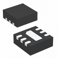
LTC3025EDC#TRMPBF Linear Technology, LTC3025EDC#TRMPBF Datasheet - Page 6

LTC3025EDC#TRMPBF
Manufacturer Part Number
LTC3025EDC#TRMPBF
Description
IC REG VLDO 300MA MICROPWR 6DFN
Manufacturer
Linear Technology
Datasheet
1.LTC3025EDCTR.pdf
(12 pages)
Specifications of LTC3025EDC#TRMPBF
Regulator Topology
Positive Adjustable
Voltage - Output
0.4 ~ 3.6 V
Voltage - Input
0.9 ~ 5.5 V
Voltage - Dropout (typical)
0.045V @ 300mA
Number Of Regulators
1
Current - Output
300mA (Min)
Operating Temperature
-40°C ~ 125°C
Mounting Type
Surface Mount
Package / Case
6-DFN
Lead Free Status / RoHS Status
Lead free / RoHS Compliant
Current - Limit (min)
-
Other names
LTC3025EDC#PBF
LTC3025EDC#PBF
LTC3025EDC#PBF
Available stocks
Company
Part Number
Manufacturer
Quantity
Price
APPLICATIONS INFORMATION
LTC3025
BLOCK DIAGRAM
Operation (Refer to Block Diagram)
The LTC3025 is a micropower, VLDO (very low dropout)
linear regulator which operates from input voltages as
low as 0.9V. The device provides a high accuracy output
that is capable of supplying 300mA of output current with
a typical dropout voltage of only 45mV. A single ceramic
capacitor as small as 1μF is all that is required for output
bypassing. A low reference voltage allows the LTC3025
output to be programmed to much lower voltages than
available in common LDOs (range of 0.4V to 3. 6V).
As shown in the Block Diagram, the BIAS input supplies
the internal reference and LDO circuitry while all output
current comes directly from the IN input for high effi ciency
regulation. The low quiescent supply currents I
I
shutdown making the LTC3025 an ideal choice for use in
battery-powered systems.
The device includes current limit and thermal overload
protection. The fast transient response of the follower
output stage overcomes the traditional tradeoff between
dropout voltage, quiescent current and load transient
response inherent in most LDO regulator architectures.
The LTC3025 also includes overshoot detection circuitry
which brings the output back into regulation when going
from heavy to light output loads (see Figure 1).
6
BIAS
= 50μA drop to I
IN
= 1μA, I
1
6
2
BIAS
SHDN
GND
BIAS
= 0.01μA typical in
SHDN
REFERENCE
0.4V
IN
= 4μA,
SOFT-START
Adjustable Output Voltage
The output voltage is set by the ratio of two external resis-
tors as shown in Figure 2. The device servos the output
to maintain the ADJ pin voltage at 0.4V (referenced to
ground). Thus the current in R1 is equal to 0.4V/R1. For
good transient response, stability, and accuracy, the current
in R1 should be at least 8μA, thus the value of R1 should
be no greater than 50k. The current in R2 is the current in
R1 plus the ADJ pin bias current. Since the ADJ pin bias
current is typically <10nA, it can be ignored in the output
voltage calculation. The output voltage can be calculated
+
–
I
OUT
20mV/DIV
300mA
V
0mA
OUT
AC
6μA
V
V
V
C
Figure 1. LTC3025 Transient Response
IN
OUT
BIAS
OUT
= 1.5V
= 1.2V
= 1μF
= 3.6V
OUT
ADJ
IN
3025 BD
100μs/DIV
3
4
5
3025 F01
3025fd


