LTC3025EDC#TRMPBF Linear Technology, LTC3025EDC#TRMPBF Datasheet - Page 5
LTC3025EDC#TRMPBF
Manufacturer Part Number
LTC3025EDC#TRMPBF
Description
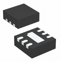
IC REG VLDO 300MA MICROPWR 6DFN
Manufacturer
Linear Technology
Datasheet
1.LTC3025EDCTR.pdf
(12 pages)
Specifications of LTC3025EDC#TRMPBF
Regulator Topology
Positive Adjustable
Voltage - Output
0.4 ~ 3.6 V
Voltage - Input
0.9 ~ 5.5 V
Voltage - Dropout (typical)
0.045V @ 300mA
Number Of Regulators
1
Current - Output
300mA (Min)
Operating Temperature
-40°C ~ 125°C
Mounting Type
Surface Mount
Package / Case
6-DFN
Lead Free Status / RoHS Status
Lead free / RoHS Compliant
Current - Limit (min)
-
Other names
LTC3025EDC#PBF
LTC3025EDC#PBF
LTC3025EDC#PBF
Available stocks
Company
Part Number
Manufacturer
Quantity
Price


TYPICAL PERFORMANCE CHARACTERISTICS
PIN FUNCTIONS
BIAS (Pin 1): BIAS Input Voltage. BIAS provides internal
power for LTC3025 circuitry. The BIAS pin should be lo-
cally bypassed to ground if the LTC3025 is more than a
few inches away from another source of bulk capacitance.
In general, the output impedance of a battery rises with
frequency, so it is usually advisable to include an input
bypass capacitor in battery-powered circuits. A capacitor
in the range of 0.01μF to 0.1μF is usually suffi cient.
GND (Pin 2): Ground. Connect to a ground plane.
IN (Pin 3): Input Supply Voltage. The output load current
is supplied directly from IN. The IN pin should be locally
bypassed to ground if the LTC3025 is more than a few inches
away from another source of bulk capacitance. In general,
the output impedance of a battery rises with frequency, so
it is usually advisable to include an input bypass capacitor
when supplying IN from a battery. A capacitor in the range
of 0.1μF to 1μF is usually suffi cient.
OUT (Pin 4): Regulated Output Voltage. The OUT pin
supplies power to the load. A minimum ceramic output
50
45
40
35
30
25
20
15
10
5
0
1.2
3MHz V
V
V
BIAS
OUT
1.4
= 1.2V
= 3.6V
IN
1.6
Supply Rejection
1.8
V
C
C
IN
OUT
OUT
(V)
2.0
= 10μF
= 1μF
I
I
2.2
OUT
OUT
= 100mA
= 300mA
2.4
3025 G12
2.6
capacitor of at least 1μF is required to ensure stability.
Larger output capacitors may be required for applications
with large transient loads to limit peak voltage transients.
See the Applications Information section for more informa-
tion on output capacitance.
ADJ (Pin 5): Adjust Input. This is the input to the error
amplifi er. The ADJ pin reference voltage is 0.4V referenced
to ground. The output voltage range is 0.4V to 3.6V and is
typically set by connecting ADJ to a resistor divider from
OUT to GND. See Figure 2.
SHDN (Pin 6): Shutdown Input, Active Low. This pin is
used to put the LTC3025 into shutdown. The SHDN pin
current is typically less than 10nA. The SHDN pin cannot
be left fl oating and must be tied to a valid logic level (such
as BIAS) if not used.
GND (Exposed Pad Pin 7): Ground and Heat Sink. Must
be soldered to PCB ground plane or large pad for optimal
thermal performance.
I
OUT
10mV/DIV
250mA
10mA
V
OUT
AC
Transient Response
V
V
V
C
IN
OUT
BIAS
OUT
= 1.5V
= 1.2V
= 1μF
= 3.6V
100μs/DIV
3025 G13
LTC3025
3025fd
5
Related parts for LTC3025EDC#TRMPBF
Image
Part Number
Description
Manufacturer
Datasheet
Request
R

Part Number:
Description:
Manufacturer:
Linear Technology Corporation
Datasheet:

Part Number:
Description:
IC, LDO VOLT REG, 1.2V, 0.5A, DFN-6
Manufacturer:
Linear Technology

Part Number:
Description:
IC REG VLDO 300MA MICROPWR 6DFN
Manufacturer:
Linear Technology
Datasheet:
Part Number:
Description:
IC REG VLDO 300MA MICROPWR 6DFN
Manufacturer:
Linear Technology
Datasheet:
Part Number:
Description:
IC REG VLDO 300MA MICROPWR 6DFN
Manufacturer:
Linear Technology
Datasheet:
Part Number:
Description:
IC REG VLDO 300MA MICROPWR 6DFN
Manufacturer:
Linear Technology
Part Number:
Description:
IC REG VLDO 500MA MICROPWR 6DFN
Manufacturer:
Linear Technology
Part Number:
Description:
IC REG VLDO 500MA MICROPWR 6DFN
Manufacturer:
Linear Technology
Datasheet:
Part Number:
Description:
IC REG VLDO 500MA MICROPWR 6DFN
Manufacturer:
Linear Technology
Part Number:
Description:
IC VLDO REG 1.5V 500MA 6-DFN
Manufacturer:
Linear Technology
Part Number:
Description:
IC VLDO REG 1.5V 500MA 6-DFN
Manufacturer:
Linear Technology
Part Number:
Description:
IC VLDO REG 1.8V 500MA 6-DFN
Manufacturer:
Linear Technology
Part Number:
Description:
IC VLDO REG 1.8V 500MA 6-DFN
Manufacturer:
Linear Technology
Part Number:
Description:
DP-LINREG, 1.2V, 500 MA Micropower, VLDO Linear Regulator
Manufacturer:
Linear Technology
Part Number:
Description:
300ma Micropower Vldo Linear Regulator
Manufacturer:
Linear Technology Corporation
Datasheet: