LTC3025EDC-2#TRMPBF Linear Technology, LTC3025EDC-2#TRMPBF Datasheet

IC REG VLDO 500MA MICROPWR 6DFN

LTC3025EDC-2#TRMPBF

Manufacturer Part Number
LTC3025EDC-2#TRMPBF
Description
IC REG VLDO 500MA MICROPWR 6DFN
Manufacturer
Linear Technology
Datasheet

Specifications of LTC3025EDC-2#TRMPBF

Regulator Topology
Positive Fixed
Voltage - Output
1.2V
Voltage - Input
Up to 5.5V
Voltage - Dropout (typical)
0.045V @ 300mA
Number Of Regulators
1
Current - Output
500mA (Min)
Operating Temperature
-40°C ~ 85°C
Mounting Type
Surface Mount
Package / Case
6-DFN
Primary Input Voltage
5.5V
Output Voltage Fixed
3.6V
Dropout Voltage Vdo
45mV
No. Of Pins
6
Output Current
500mA
Voltage Regulator Case Style
DFN
Operating Temperature Range
-40°C To +125°C
Rohs Compliant
Yes
Lead Free Status / RoHS Status
Lead free / RoHS Compliant
Current - Limit (min)
-

Available stocks

Company
Part Number
Manufacturer
Quantity
Price
Company:
Part Number:
LTC3025EDC-2#TRMPBFLTC3025EDC-2
Manufacturer:
LT
Quantity:
10 000
FEATURES
APPLICATIONS
n
n
n
n
n
n
n
n
n
n
n
n
n
n
n
n
n
n
n
n
n
TYPICAL APPLICATION
3-CELL
Li-Ion
NiMH
OR
Wide Input Voltage Range: 0.9V to 5.5V
Stable with Ceramic Capacitors
Very Low Dropout: 45mV at 300mA
Adjustable Output Range: 0.4V to 3.6V
±2% Voltage Accuracy over Temperature
Supply Load
Low Noise: 80μV
BIAS Voltage Range: 2.5V to 5.5V
Fast Transient Recovery
Shutdown Disconnects Load from V
Low Operating Current: I
Low Shutdown Current: I
Output Current Limit
Thermal Overload Protection
Available in 6-Lead (2mm × 2mm) DFN Package
Low Power Handheld Devices
Low Voltage Logic Supplies
DSP Power Supplies
Cellular Phones
Portable Electronic Equipment
Handheld Medical Instruments
Post Regulator for Switching Supply Noise Rejection
EFFICIENCY
1.5V HIGH
DC/DC
BUCK
1.2V Output Voltage from 1.5V Input Supply
1.5V
RMS
OFF ON
0.1μF
0.1μF
(10Hz to 100kHz)
IN
IN
BIAS
IN
SHDN
= 4μA, I
= 1μA, I
LTC3025
GND
OUT
ADJ
BIAS
BIAS
IN
and V
= 50μA Typ
= 0.01μA Typ
80.6k
40.2k
3025 TA01
BIAS
1μF
V
I
OUT
OUT
≤ 300mA
= 1.2V
DESCRIPTION
The LTC
out) linear regulator which operates from input voltages as
low as 0.9V. The device is capable of supplying 300mA of
output current with a typical dropout voltage of only 45mV.
A BIAS supply is required to run the internal reference and
LDO circuitry while output current comes directly from
the IN supply for high effi ciency regulation. The low 0.4V
internal reference voltage allows the LTC3025 output to
be programmed to much lower voltages than available in
common LDOs (range of 0.4V to 3.6V). The output voltage
is programmed via two ultrasmall SMD resistors.
The LTC3025’s low quiescent current makes it an ideal
choice for use in battery-powered systems. For 3-cell
NiMH and single cell Li-Ion applications, the BIAS voltage
can be supplied directly from the battery while the input
can come from a high effi ciency buck regulator, providing
a high effi ciency, low noise output.
Other features include high output voltage accuracy,
excellent transient response, stability with ultralow ESR
ceramic capacitors as small as 1μF , short-circuit and
thermal overload protection and output current limiting.
The LTC3025 is available in a tiny, low profi le (0.75mm)
6-lead DFN (2mm × 2mm) package.
L, LT, LTC and LTM are registered trademarks of Linear Technology Corporation.
VLDO is a trademark of Linear Technology Corporation.
All other trademarks are the property of their respective owners.
VLDO Linear Regulator
®
3025 is a micropower, VLDO
50
45
40
35
30
25
20
15
10
300mA Micropower
5
0
1.2
1MHz V
BIAS = 3.6V
V
OUT
1.4
= 1.2V
IN
1.6
Supply Rejection
C
C
OUT
1.8
OUT
V
IN
= 10μF
= 1μF
(V)
2.0
I
I
2.2
OUT
OUT
= 100mA
= 300mA
TM
2.4
LTC3025
3025 TA01b
(very low drop-
2.6
3025fb
1

Related parts for LTC3025EDC-2#TRMPBF

LTC3025EDC-2#TRMPBF Summary of contents

Page 1

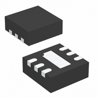
... The LTC3025 is available in a tiny, low profi le (0.75mm) 6-lead DFN (2mm × 2mm) package. L, LT, LTC and LTM are registered trademarks of Linear Technology Corporation. VLDO is a trademark of Linear Technology Corporation. All other trademarks are the property of their respective owners. ...

Page 2

... LTC3025IDC#PBF LTC3025IDC#TRPBF LEAD BASED FINISH TAPE AND REEL LTC3025EDC LTC3025EDC#TR LTC3025IDC LTC3025IDC#TR Consult LTC Marketing for parts specifi ed with wider operating temperature ranges. *The temperature grade is identifi label on the shipping container. For more information on lead free part marking, go to: For more information on tape and reel specifi ...

Page 3

ELECTRICAL CHARACTERISTICS temperature range, otherwise specifi cations are 0.1μF (all capacitors ceramic) unless otherwise noted. BIAS PARAMETER BIAS Line Regulation (Referred to ADJ Pin Dropout Voltage (Notes OUT V ...

Page 4

LTC3025 TYPICAL PERFORMANCE CHARACTERISTICS Dropout Voltage vs I OUT 2.8V BIAS 125° 25° –40° 100 150 200 250 I ...

Page 5

TYPICAL PERFORMANCE CHARACTERISTICS V Ripple Rejection IN vs Frequency OUT 3.6V BIAS 1.2V OUT I = 100mA OUT 0 100 1k 10k 100k FREQUENCY ...

Page 6

LTC3025 PIN FUNCTIONS BIAS (Pin 1): BIAS Input Voltage. BIAS provides internal power for LTC3025 circuitry. The BIAS pin should be lo- cally bypassed to ground if the LTC3025 is more than a few inches away from another source of ...

Page 7

APPLICATIONS INFORMATION Operation (Refer to Block Diagram) The LTC3025 is a micropower, VLDO (very low dropout) linear regulator which operates from input voltages as low as 0.9V. The device provides a high accuracy output that is capable of supplying 300mA ...

Page 8

LTC3025 APPLICATIONS INFORMATION Output Capacitance and Transient Response The LTC3025 is designed to be stable with a wide range of ceramic output capacitors. The ESR of the output capaci- tor affects stability, most notably with small capacitors. A minimum output ...

Page 9

APPLICATIONS INFORMATION The LTC3025 2mm × 2mm DFN package is specifi hav- ing a junction-to-ambient thermal resistance of 102°C/W, which assumes a minimal heat spreading copper plane. The actual thermal resistance can be reduced substantially by connecting the ...

Page 10

LTC3025 TYPICAL APPLICATION High Effi ciency 1.5V Step-Down Converter with Effi cient 1.2V VLDO Output OFF 2. 5. 4.7μF LTC3406-1.5 CER 1 RUN * MURATA LQH32CN2R2M33 ** TAIYO YUDEN JMK212BJ475MG ...

Page 11

... SHADED AREA IS ONLY A REFERENCE FOR PIN 1 LOCATION ON THE TOP AND BOTTOM OF PACKAGE Information furnished by Linear Technology Corporation is believed to be accurate and reliable. However, no responsibility is assumed for its use. Linear Technology Corporation makes no representa- tion that the interconnection of its circuits as described herein will not infringe on existing patent rights. DC Package 6-Lead Plastic DFN (2mm × ...

Page 12

... LT3020 100mA, Low Voltage, VLDO LT3023 Dual, 2 × 100mA, Low Noise Micropower, LDO LT3024 Dual 100mA/500mA, Low Noise Micropower, LDO ThinSOT is a trademark of Linear Technology Corporation. Linear Technology Corporation 12 1630 McCarthy Blvd., Milpitas, CA 95035-7417 (408) 432-1900 FAX: (408) 434-0507 ● COMMENTS ...

Related keywords