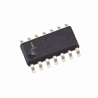
X5643S14-2.7 Intersil, X5643S14-2.7 Datasheet - Page 6

X5643S14-2.7
Manufacturer Part Number
X5643S14-2.7
Description
IC CPU SUPRV 64K EE RST LO SO14
Manufacturer
Intersil
Type
Simple Reset/Power-On Resetr
Datasheet
1.X5643P.pdf
(19 pages)
Specifications of X5643S14-2.7
Number Of Voltages Monitored
1
Output
Open Drain or Open Collector
Reset
Active Low
Reset Timeout
100 ms Minimum
Voltage - Threshold
2.63V
Operating Temperature
0°C ~ 70°C
Mounting Type
Surface Mount
Package / Case
14-SOIC (3.9mm Width), 14-SOL
Lead Free Status / RoHS Status
Contains lead / RoHS non-compliant
Table 2. Block Protect Matrix
The Write Enable Latch (WEL) bit indicates the sta-
tus of the write enable latch. When WEL = 1, the
latch is set HIGH and when WEL = 0 the latch is reset
LOW. The WEL bit is a volatile, read only bit. It can
be set by the WREN instruction and can be reset by
the WRDS instruction.
The block lock bits, BL0 and BL1, set the level of block
lock protection. These nonvolatile bits are pro-
grammed using the WRSR instruction and allow the
user to protect one quarter, one half, all or none of the
EEPROM array. Any portion of the array that is block
lock protected can be read but not written. It will
remain protected until the BL bits are altered to disable
block lock protection of that portion of memory.
The watchdog timer bits, WD0 and WD1, select the
watchdog time out period. These nonvolatile bits are
programmed with the WRSR instruction.
WREN CMD
Register Bits
BL1
0
0
1
1
WEL
Status
0
1
1
1
BL0
0
1
0
1
Status Register
Array Addresses Protected
WPEN
X
X
1
0
6
X5643/X5645
$1800-$1FFF
$1000-$1FFF
$0000-$1FFF
None
Device Pin
WP#
X
X
0
1
X5643, X5645
Protected Block
Protected
Protected
Protected
Protected
Block
The FLAG bit shows the status of a volatile latch that
can be set and reset by the system using the SFLB
and RFLB instructions. The flag bit is automatically
reset upon power-up. This flag can be used by the sys-
tem to determine whether a reset occurs as a result of
a watchdog time out or power failure.
The nonvolatile WPEN bit is programmed using the
WRSR instruction. This bit works in conjunction with the
WP pin to provide an in-circuit programmable ROM func-
tion (Table 2). WP is LOW and WPEN bit programmed
HIGH disables all status register write operations.
In Circuit Programmable ROM Mode
This mechanism protects the block lock and watchdog
bits from inadvertent corruption.
In the locked state (
is LOW and the nonvolatile bit WPEN is “1”. This mode
disables nonvolatile writes to the device’s status register.
Status Register Bits
WD1
0
0
1
1
Unprotected Block
Protected
Writable
Writable
Writable
Block
programmable ROM mode) the WP pin
WD0
0
1
0
1
Watchdog Time Out
600 milliseconds
200 milliseconds
WPEN, BL0, BL1
Status Register
1.4 seconds
(Typical)
disabled
WD0, WD1
Protected
Protected
Writable
Writable
July 18, 2005
FN8135.1


