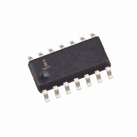
X5643S14-2.7 Intersil, X5643S14-2.7 Datasheet - Page 3

X5643S14-2.7
Manufacturer Part Number
X5643S14-2.7
Description
IC CPU SUPRV 64K EE RST LO SO14
Manufacturer
Intersil
Type
Simple Reset/Power-On Resetr
Datasheet
1.X5643P.pdf
(19 pages)
Specifications of X5643S14-2.7
Number Of Voltages Monitored
1
Output
Open Drain or Open Collector
Reset
Active Low
Reset Timeout
100 ms Minimum
Voltage - Threshold
2.63V
Operating Temperature
0°C ~ 70°C
Mounting Type
Surface Mount
Package / Case
14-SOIC (3.9mm Width), 14-SOL
Lead Free Status / RoHS Status
Contains lead / RoHS non-compliant
PRINCIPLES OF OPERATION
Power-on Reset
Application of power to the X5643/X5645 activates a
power-on reset circuit. This circuit goes active at about
1V and pulls the RESET/RESET pin active. This signal
prevents the system microprocessor from starting to
operate with insufficient voltage or prior to stabilization
of the oscillator. When V
value for 200ms (nominal) the circuit releases
RESET/RESET, allowing the processor to begin execut-
ing code.
Low Voltage Monitoring
During operation, the X5643/X5645 monitors the V
level and asserts RESET/RESET if supply voltage falls
below a preset minimum V
signal prevents the microprocessor from operating in a
power fail or brownout condition. The RESET/RESET
signal remains active until the voltage drops below 1V.
It also remains active until V
V
Watchdog Timer
The watchdog timer circuit monitors the microprocessor
activity by monitoring the WDI input. The microproces-
sor must toggle the CS/WDI pin periodically to prevent a
RESET/RESET signal. The CS/WDI pin must be toggled
from HIGH to LOW prior to the expiration of the watch-
dog time out period. The state of two nonvolatile con-
trol bits in the status register determine the watchdog
timer period. The microprocessor can change these
watchdog bits, or they may be “locked” by tying the WP
pin LOW and setting the WPEN bit HIGH.
V
The X5643/X5645 has a standard V
(V
operating and storage conditions. However, in applica-
tions where the standard V
for
X5643/X5645 threshold may be adjusted.
Setting the V
This procedure sets the V
value. For example, if the current V
new V
change. If the new setting is lower than the current set-
ting, then it is necessary to reset the trip point before
setting the new value.
TRIP
CC
TRIP
Threshold Reset Procedure
higher
for 200ms.
) voltage. This value will not change over normal
TRIP
is 4.6V, this procedure directly makes the
precision
TRIP
Voltage
CC
in
3
TRIP
TRIP
TRIP
exceeds the device V
the
CC
. The RESET/RESET
is not exactly right, or
returns and exceeds
to a higher voltage
TRIP
V
TRIP
is 4.4V and the
CC
value,
threshold
X5643, X5645
TRIP
the
CC
To set the new V
threshold to the Vcc pin and tie the CS/WDI pin and
the WP pin HIGH. RESET/RESET and SO pins are
left unconnected. Then apply the programming voltage
V
HIGH. Remove V
Figure 1. Set V
Resetting the V
This procedure sets the V
level. For example, if the current V
V
1.7V. This procedure must be used to set the voltage
to a lower value.
To reset the V
and 5.5V to the V
and the SCK pin HIGH. RESET/RESET and SO pins are
left unconnected. Then apply the programming voltage
V
HIGH. Remove V
Figure 2. Reset V
P
TRIP
P
to both SCK and SI and pulse CS/WDI LOW then
to the SI pin ONLY and pulse CS/WDI LOW then
is reset, the new V
SCK
SCK
SI
CS
SI
CS
V
V
V
V
TRIP
P
CC
P
P
TRIP
TRIP
CC
P
TRIP
P
and the sequence is complete.
TRIP
voltage, apply a voltage between 2.7
and the sequence is complete.
pin. Tie the CS/WDI pin, the WP pin,
Voltage
Voltage
voltage, apply the desired V
Voltage
TRIP
TRIP
is something less than
to a “native” voltage
TRIP
is 4.4V and the
July 18, 2005
FN8135.1
TRIP


