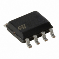
STM690SM6F STMicroelectronics, STM690SM6F Datasheet - Page 16

STM690SM6F
Manufacturer Part Number
STM690SM6F
Description
SUPERVISOR 3V SWITCH OVER 8SOIC
Manufacturer
STMicroelectronics
Type
Simple Reset/Power-On Resetr
Datasheet
1.STM704RM6F.pdf
(42 pages)
Specifications of STM690SM6F
Number Of Voltages Monitored
1
Output
Push-Pull, Totem Pole
Reset
Active Low
Reset Timeout
140 ms Minimum
Voltage - Threshold
2.925V
Operating Temperature
-40°C ~ 85°C
Mounting Type
Surface Mount
Package / Case
8-SOIC (3.9mm Width)
Monitored Voltage
1 V to 5.5 V
Manual Reset
Not Resettable
Watchdog
Watchdog
Battery Backup Switching
Backup
Supply Voltage (max)
5.5 V
Supply Voltage (min)
1 V
Supply Current (typ)
60 uA
Maximum Power Dissipation
320 mW
Maximum Operating Temperature
+ 85 C
Mounting Style
SMD/SMT
Minimum Operating Temperature
- 40 C
Power Fail Detection
Yes
Threshold Voltage
2.935V
No. Of Supervisors / Monitors
1
Supply Voltage Range
1.1V To 5.5V
Reset Type
Active-Low
Supply Current
40µA
Delay Time
200ms
Digital Ic Case Style
SOIC
Rohs Compliant
Yes
Undervoltage Threshold
2.85 V
Overvoltage Threshold
3 V
Output Type
Active Low
Power-up Reset Delay (typ)
280 ms
Lead Free Status / RoHS Status
Lead free / RoHS Compliant
Other names
497-3826-2
Available stocks
Company
Part Number
Manufacturer
Quantity
Price
Operation
2.5
2.6
2.7
Figure 11. Chip enable gating
16/42
V CC
E
V RST
Chip enable gating (STM795 only)
Internal gating of the chip enable (E) signal prevents erroneous data from corrupting the
external CMOS RAM in the event of an undervoltage condition. The STM795 uses a series
transmission gate from E to E
asserted), the E transmission gate is enabled and passes all E transitions. When reset is
asserted, this path becomes disabled, preventing erroneous data from corrupting the CMOS
RAM. The short E propagation delay from E to E
most µPs. If E is low when reset asserts, E
current write cycle to complete.
Chip enable input (STM795 only)
The chip enable transmission gate is disabled and E is high impedance (disabled mode)
while reset is asserted. During a power-down sequence when V
threshold, the chip enable transmission gate disables and E immediately becomes high
impedance if the voltage at E is high. If E is low when reset asserts, the chip enable
transmission gate will disable 10 µs after reset asserts (see
current write cycle to complete during power-down.
Any time a reset is generated, the chip enable transmission gate remains disabled and E
remains high impedance (regardless of E activity) for the first half of the reset time-out
period (t
appears as a 40
the chip enable transmission gate depends on V
connected to E, and the loading on E
tested from the 50% point on E to the 50% point on E
load capacitance (see
load at E
Chip enable output (STM795 only)
When the chip enable transmission gate is enabled, the impedance of E
a 40
gate is off and an active pull-up connects E
off when the transmission gate is enabled.
resistor in series with the source driving E. In the disabled mode, the transmission
rec
CON
/2). When the chip enable transmission gate is enabled, the impedance of E
and use a low-output impedance driver.
resistor in series with the load at E
Figure
STM690, STM704, STM795, STM802, STM804, STM805, STM806
COMPARE
CON
35). For minimum propagation delay, minimize the capacitive
Doc ID 10519 Rev 9
(see
E CON OUTPUT
CONTROL
CON
Figure
. The chip enable propagation delay is production
CON
CON
11). During normal operation (reset not
remains low for typically 10 µs to permit the
to V
CC
CON
, the source impedance of the drive
OUT
enables the STM795 to be used with
CON
CON
generator
(see
t rec
. The propagation delay through
using a 50
Figure
Figure
CC
12). This permits the
passes the reset
11). This pull-up turns
CON
driver and a 50 pF
is equivalent to
RST
V OUT
E CON
AI08802


