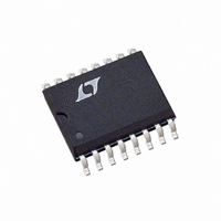
LTC695CSW-3.3#PBF Linear Technology, LTC695CSW-3.3#PBF Datasheet - Page 5

LTC695CSW-3.3#PBF
Manufacturer Part Number
LTC695CSW-3.3#PBF
Description
IC MPU SUPRVSRY CIRC 3.3V 16SOIC
Manufacturer
Linear Technology
Type
Simple Reset/Power-On Resetr
Datasheet
1.LTC694CS8-3.3PBF.pdf
(20 pages)
Specifications of LTC695CSW-3.3#PBF
Number Of Voltages Monitored
1
Output
Open Drain or Open Collector
Reset
Active High/Active Low
Reset Timeout
140 ms Minimum
Voltage - Threshold
2.9V
Operating Temperature
0°C ~ 70°C
Mounting Type
Surface Mount
Package / Case
16-SOIC (0.300", 7.5mm Width)
Lead Free Status / RoHS Status
Lead free / RoHS Compliant
Available stocks
Company
Part Number
Manufacturer
Quantity
Price
ELECTRICAL CHARACTERISTICS
temperature range, otherwise specifications are at T
PARAMETER
Power-Fail Detector
PFI Input Threshold
PFI Input Threshold PSRR
PFI Input Current
PFO Output Voltage (Note 4)
PFO Short-Circuit Source Current (Note 4)
PFI Comparator Response Time (Falling)
PFI Comparator Response Time (Rising) (Note 4)
Chip Enable Gating
CE IN Threshold
CE IN Pull-Up Current (Note 6)
CE OUT Output Voltage
CE IN Propagation Delay
CE OUT Output Short-Circuit Current
Oscillator
OSC IN Input Current (Note 6)
OSC SEL Input Pull-Up Current (Note 6)
OSC IN Frequency Range
Note 1: Stresses beyond those listed under Absolute Maximum Ratings
may cause permanent damage to the device. Exposure to any Absolute
Maximum Rating condition for extended periods may affect device
reliability and lifetime.
Note 2: All voltage values are with respect to GND.
Note 3: For military temperature range parts, consult the factory.
Note 4: The output pins of BATT ON, LOW
RESET have weak internal pull-ups of typically 3μA. However, external pull-
up resistors may be used when higher speed is required.
_
LINE, PFO, WDO, RESET and
CONDITIONS
I
PFI = LOW, PFO = V
with 10kΩ Pull-Up
V
V
I
I
C
Output Sink Current
OSC SEL = 0V, C
I
PFI = HIGH, PFO = 0V
ΔV
ΔV
I
Output Source Current
OSC SEL = 0V
SINK
SOURCE
SINK
SOURCE
SOURCE
IL
IH
L
IN
IN
= 20pF
= –20mV, V
= 20mV, V
= 800μA
= 800μA
A
= 25°C. V
= 0.1μA
= 400μA
= 1μA, V
The
OD
OD
A
CC
l
= 47pF
= 15mV
CC
= 15mV
OUT
= 0V
denotes the specifications which apply over the full operating
= 3.3V, V
Note 5: The external clock feeding into the circuit passes through the
oscillator before clocking the watchdog timer. Variation in the timeout
period is caused by phase errors which occur when the oscillator divides
the external clock by 64. The resulting variation in the timeout period is 64
plus one clock of jitter.
Note 6: The input pins of CE IN, OSC IN and OSC SEL have weak internal
pull-ups which pull to the supply when the input pins are floating.
BATT
= 2V, unless otherwise noted.
LTC694-3.3/LTC695-3.3
l
l
l
l
l
l
l
l
l
l
V
V
OUT
OUT
MIN
1.25
2.3
1.9
1
0
– 0.50
– 0.05
±0.01
TYP
1.3
0.3
17
40
30
15
20
±2
3
2
8
3
5
4
MAX
1.35
0.45
±25
125
0.3
0.3
25
50
UNITS
69453fb
mV/V
5
kHz
kHz
mA
mA
nA
μA
μA
μA
μA
μA
μs
μs
μs
ns
V
V
V
V
V
V
V
V


