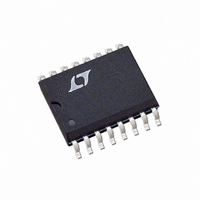
LTC695CSW-3.3#PBF Linear Technology, LTC695CSW-3.3#PBF Datasheet - Page 13

LTC695CSW-3.3#PBF
Manufacturer Part Number
LTC695CSW-3.3#PBF
Description
IC MPU SUPRVSRY CIRC 3.3V 16SOIC
Manufacturer
Linear Technology
Type
Simple Reset/Power-On Resetr
Datasheet
1.LTC694CS8-3.3PBF.pdf
(20 pages)
Specifications of LTC695CSW-3.3#PBF
Number Of Voltages Monitored
1
Output
Open Drain or Open Collector
Reset
Active High/Active Low
Reset Timeout
140 ms Minimum
Voltage - Threshold
2.9V
Operating Temperature
0°C ~ 70°C
Mounting Type
Surface Mount
Package / Case
16-SOIC (0.300", 7.5mm Width)
Lead Free Status / RoHS Status
Lead free / RoHS Compliant
Available stocks
Company
Part Number
Manufacturer
Quantity
Price
APPLICATIONS INFORMATION
Example 1: The circuit in Figure 8 demonstrates the use
of the power-fail comparator to monitor the unregulated
power supply input. Assuming the the rate of decay of the
supply input V
shutdown procedure is 8ms. Also the noise of V
With these assumptions in mind, we can reasonably set
V
reset voltage threshold and the dropout voltage of the
LT1129-3.3 (3V + 0.4V) and V
Choose R3 = 200k and R1 = 51k. Also select R4 = 10k
which is much smaller than R3.
R2 = 15.8k, Choose nearest 5% resistor 16k and recal-
culate V
The 15.6ms allows enough time to execute shutdown pro-
cedure for microprocessor and 810mV of hysteresis would
prevent PFO from going low due to the noise of V
Example 2: The circuit in Figure 9 can be used to measure
the regulated 3.3V supply to provide early warning of
power failure. Because of variations in the PFI threshold,
this circuit requires adjustment to ensure the PFI compara-
tor trips before the reset threshold is reached. Adjust R5
such that the PFO output goes low when the V
reaches the desired level (e.g., 3.1V).
L
R3 ≈ 3.88 R1
V
= 5V which is 1.6V greater than the sum of maximum
5V =1.3V 1−
V
V
V
(4.96V − 3.4V)
HYSTERESIS
HYSTERESIS
L
H
100mV / ms
= 1.3V 1+
= 1.3V 1+
L
,
IN
⎛
⎝ ⎜
⎛
⎝ ⎜
⎛
⎝ ⎜
= 5.77V – 4.96V = 810mV
is 100mV/ms and the total time to execute a
= 3.3V
51k
51k
16k
16 k
R2
51k
= 15.6ms
−
−
R3
+
R1
(3.3V −1.3V)51k
(3.3V − 1.3V)51k
2 00k
51k
= 850mV
1.3V(210k)
1.3V(210k)
HYSTERESIS
⎞
⎠ ⎟
= 5.77 V
= 850mV.
⎞
⎠ ⎟
⎞
⎠ ⎟
= 4.96 V
IN
CC
is 200mV.
IN
supply
.
Monitoring the Status of the Battery
C3 can also monitor the status of the memory back-up
battery (Figure 10). If desired, the CE OUT can be used to
apply a test load to the battery. Since CE OUT is forced high
in battery back-up mode, the test load will not be applied
to the battery while it is in use, even if the microprocessor
is not powered.
Watchdog Timer
The LTC694-3.3/LTC695-3.3 provide a watchdog timer
function to monitor the activity of the microprocessor. If
the microprocessor does not toggle the watchdog input
(WDI) within a selected timeout period, RESET is forced
to active low for a minimum of 140ms. The reset active
time is adjustable on the LTC695-3.3. Since many systems
can not service the watchdog timer immediately after a
reset, the LTC695-3.3 has a longer timeout period (1.0
second minimum) right after a reset is issued. The normal
timeout period (70ms minimum) becomes effective follow-
ing the first transition of WDI after RESET is inactive. The
watchdog timeout period is fixed at 1.0 second minimum
on the LTC694-3.3. Figure 11 shows the timing diagram
of watchdog timeout period and reset active time. The
watchdog timeout period is restarted as soon as RESET is
inactive. When either a high-to-low or low-to-high transi-
tion occurs at the WDI pin prior to timeout, the watchdog
time is reset and begins to time out again. To ensure the
watchdog time does not time out, either a high-to-low or
low-to-high transition on the WDI pin must occur at or
less than the minimum timeout period. If the input to the
Figure 10. Back-Up Battery Monitor with Optional Test Load
2.4V
OPTIONAL TEST LOAD
LTC694-3.3/LTC695-3.3
R1
1M
R2
1.6M
20k
R
L
V
PFI
CE OUT
BATT
LTC695-3.3
3.3V
V
CC
GND
CE IN
PFO
LOW-BATTERY SIGNAL
T0 μP I/O PIN
I/O PIN
694/5-3.3 F10
13
69453fb


