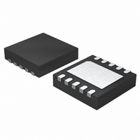
LT1995IDD#PBF Linear Technology, LT1995IDD#PBF Datasheet - Page 2

LT1995IDD#PBF
Manufacturer Part Number
LT1995IDD#PBF
Description
IC AMP GAIN SELECT 10-DFN
Manufacturer
Linear Technology
Datasheet
1.LT1995CMSPBF.pdf
(20 pages)
Specifications of LT1995IDD#PBF
Amplifier Type
Programmable Gain
Number Of Circuits
1
Slew Rate
1000 V/µs
-3db Bandwidth
32MHz
Voltage - Input Offset
750µV
Current - Supply
7.1mA
Current - Output / Channel
120mA
Voltage - Supply, Single/dual (±)
5 V ~ 30 V, ±2.5 V ~ 15 V
Operating Temperature
-40°C ~ 85°C
Mounting Type
Surface Mount
Package / Case
10-WFDFN Exposed Pad
Lead Free Status / RoHS Status
Lead free / RoHS Compliant
Output Type
-
Gain Bandwidth Product
-
Current - Input Bias
-
Available stocks
Company
Part Number
Manufacturer
Quantity
Price
PACKAGE/ORDER
ABSOLUTE
Consult LTC Marketing for parts specified with wider operating temperature ranges. *The temperature grades are identified by a label on the shipping container.
LT1995
Total Supply Voltage (V
Input Current (Note 2) ....................................... ±10mA
Output Short-Circuit Duration (Note 3) ........... Indefinite
Operating Temperature Range (Note 4) .. – 40°C to 85°C
Specified Temperature Range (Note 5) ... – 40°C to 85°C
ELECTRICAL CHARACTERISTICS
2
Difference Amplifier Configuration. T
SYMBOL PARAMETER
GE
GNL
V
Order Options Tape and Reel: Add #TR
Lead Free: Add #PBF Lead Free Tape and Reel: Add #TRPBF
Lead Free Part Marking:
OS
EXPOSED PAD INTERNALLY CONNECTED TO V
T
10-LEAD (3mm × 3mm) PLASTIC DFN
JMAX
REF
V
Gain Error
Gain Nonlinearity
Input Offset Voltage
Referred to Input (Note 7)
P1
P2
P4
S
–
PCB CONNECTION OPTIONAL
= 125°C, θ
1
2
3
4
5
DD PACKAGE
TOP VIEW
JA
W
+ –
MAXIMUM
= 160°C/W (NOTE 6)
http://www.linear.com/leadfree/
+
to V
10
9
8
7
6
W W
M1
M2
M4
V
OUT
S
–
+
INFORMATION
) .............................. 36V
U
A
S
–
= 25°C, V
CONDITIONS
V
V
V
V
V
V
V
G = 1 (MS10)
G = 1 (DD10)
G = 2 (MS10)
G = 2 (DD10)
G = 4 (MS10)
G = 4 (DD10)
G = 1 (MS10)
G = 1 (DD10)
G = 1 (MS10)
G = 1 (DD10)
OUT
OUT
OUT
OUT
OUT
OUT
OUT
RATINGS
= ±12V, R
= ±12V, R
= ±12V, R
= ±5V, R
= ±2.5V, R
= ±2.5V, R
= ±12V, R
W
ORDER PART
REF
LT1995CDD
LT1995IDD
MARKING*
NUMBER
DD PART
U
= V
LBJF
LBJF
L
L
L
L
L
= 150Ω, G = 1
L
L
CM
= 1k, G = 1
= 1k, G = 2
= 1k, G = 4
= 1k, G = 1
= 500Ω, G = 1
= 150Ω, G = 1
= 0V and unused gain pins are unconnected, unless otherwise noted.
U
(Note 1)
Storage Temperature Range
Maximum Junction Temperature
Lead Temperature (Soldering, 10 sec).................. 300°C
MS Package .................................... – 65°C to 150°C
DD Package ..................................... – 65°C to 125°C
MS Package ..................................................... 150°C
DD Package ..................................................... 125°C
T
JMAX
REF
V
P1
P2
P4
S
–
10-LEAD PLASTIC MSOP
= 150°C, θ
1
2
3
4
5
V
±15V
±15V
±15V
±15V
±5V
±5V
±15V
±15V
±15V
±15V
±15V
±15V
±15V
±5V
±5V
±2.5V
±2.5V
SUPPLY
MS PACKAGE
TOP VIEW
JA
+ –
= 160°C/W (NOTE 6)
10
9
8
7
6
M1
M2
M4
V
OUT
S
+
MIN
0.05
0.05
0.05
0.05
0.05
0.05
TYP
1.5
0.7
1.2
0.6
0.9
1.4
1.3
10
1
1
1
ORDER PART
LT1995CMS
LT1995IMS
MARKING*
MS PART
NUMBER
LTBJD
LTBJD
MAX
0.25
0.25
3.75
0.2
0.2
0.2
0.2
6.8
5.6
5
9
4
5
9
5
9
UNITS
1995fb
ppm
mV
mV
mV
mV
mV
mV
mV
mV
mV
mV
%
%
%
%
%
%


