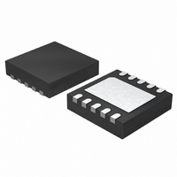
LT1995IDD#PBF Linear Technology, LT1995IDD#PBF Datasheet - Page 11

LT1995IDD#PBF
Manufacturer Part Number
LT1995IDD#PBF
Description
IC AMP GAIN SELECT 10-DFN
Manufacturer
Linear Technology
Datasheet
1.LT1995CMSPBF.pdf
(20 pages)
Specifications of LT1995IDD#PBF
Amplifier Type
Programmable Gain
Number Of Circuits
1
Slew Rate
1000 V/µs
-3db Bandwidth
32MHz
Voltage - Input Offset
750µV
Current - Supply
7.1mA
Current - Output / Channel
120mA
Voltage - Supply, Single/dual (±)
5 V ~ 30 V, ±2.5 V ~ 15 V
Operating Temperature
-40°C ~ 85°C
Mounting Type
Surface Mount
Package / Case
10-WFDFN Exposed Pad
Lead Free Status / RoHS Status
Lead free / RoHS Compliant
Output Type
-
Gain Bandwidth Product
-
Current - Input Bias
-
Available stocks
Company
Part Number
Manufacturer
Quantity
Price
BLOCK DIAGRA
APPLICATIO S I FOR ATIO
Configuration Flexibility
The LT1995 combines a high speed precision operational
amplifier with eight ratio-matched on-chip resistors. The
resistor configuration and pinout of the device is shown in
the Block Diagram. The topology is extremely versatile and
provides for simple realizations of most classic functional
configurations including difference amplifiers, inverting
gain stages, noninverting gain stages (including Hi-Z
input buffers) and summing amplifiers. The LT1995 deliv-
ers load currents of at least 30mA, making it ideal for cable
driving applications as well.
The input voltage range depends on gain and configura-
tion. ESD diodes will clamp any input voltage that exceeds
the supply potentials by more than several tenths of a volt;
and the internal op amp input ports must remain at least
1.75V within the rails to assure normal operation of the
part. The output will swing to within one and a half volts of
U
U
W
W
10
1
2
3
8
9
P1
P2
P4
M4
M2
M1
U
R
R
R
R
R
R
M1
M4
M2
P1
P2
P4
0.5pF
0.5pF
= 4k
= 2k
= 1k
= 4k
= 1k
= 2k
V
V
S
S
+
–
+
–
the rails, which in low supply voltage and high gain
configurations will create a limitation on the usable input
range. It should be noted that while the internal op amp can
withstand transient differential input voltages of up to 10V
without damage, this does generate large supply current
increases (tens of mA) as required for high slew rates. If
the device is used with sustained differential input across
the internal op amp (such as when the output is clipping),
the average supply current will increase, excessive power
dissipation will result, and the part may be damaged (i.e.,
the LT1995 is not recommended for use in comparator
applications or with the output clipped).
Difference Amplifier
The LT1995 can be connected as a classic difference
amplifier with an output function given by:
7
4
V
OUT
R
R
FB
0.3pF
0.3pF
FB
= 4k
= 4k
= G • (V
IN
OUT
REF
1995 BD
+
– V
5
6
IN
–
) + V
REF
LT1995
11
1995fb


