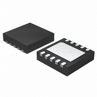
LT1995IDD#PBF Linear Technology, LT1995IDD#PBF Datasheet - Page 19

LT1995IDD#PBF
Manufacturer Part Number
LT1995IDD#PBF
Description
IC AMP GAIN SELECT 10-DFN
Manufacturer
Linear Technology
Datasheet
1.LT1995CMSPBF.pdf
(20 pages)
Specifications of LT1995IDD#PBF
Amplifier Type
Programmable Gain
Number Of Circuits
1
Slew Rate
1000 V/µs
-3db Bandwidth
32MHz
Voltage - Input Offset
750µV
Current - Supply
7.1mA
Current - Output / Channel
120mA
Voltage - Supply, Single/dual (±)
5 V ~ 30 V, ±2.5 V ~ 15 V
Operating Temperature
-40°C ~ 85°C
Mounting Type
Surface Mount
Package / Case
10-WFDFN Exposed Pad
Lead Free Status / RoHS Status
Lead free / RoHS Compliant
Output Type
-
Gain Bandwidth Product
-
Current - Input Bias
-
Available stocks
Company
Part Number
Manufacturer
Quantity
Price
PACKAGE DESCRIPTIO
3.50 ±0.05
(.0120 ± .0015)
0.305 ± 0.038
2.15 ±0.05
TYP
(.206)
5.23
MIN
RECOMMENDED SOLDER PAD PITCH AND DIMENSIONS
RECOMMENDED SOLDER PAD LAYOUT
NOTE:
1. DIMENSIONS IN MILLIMETER/(INCH)
2. DRAWING NOT TO SCALE
3. DIMENSION DOES NOT INCLUDE MOLD FLASH, PROTRUSIONS OR GATE BURRS.
4. DIMENSION DOES NOT INCLUDE INTERLEAD FLASH OR PROTRUSIONS.
5. LEAD COPLANARITY (BOTTOM OF LEADS AFTER FORMING) SHALL BE 0.102mm (.004") MAX
0.25 ± 0.05
1.65 ±0.05
(2 SIDES)
MOLD FLASH, PROTRUSIONS OR GATE BURRS SHALL NOT EXCEED 0.152mm (.006") PER SIDE
INTERLEAD FLASH OR PROTRUSIONS SHALL NOT EXCEED 0.152mm (.006") PER SIDE
2.38 ±0.05
(2 SIDES)
0.889 ± 0.127
(.035 ± .005)
(.126 – .136)
3.20 – 3.45
Information furnished by Linear Technology Corporation is believed to be accurate and reliable.
However, no responsibility is assumed for its use. Linear Technology Corporation makes no represen-
tation that the interconnection of its circuits as described herein will not infringe on existing patent rights.
(.0197)
0.50
BSC
0.50
BSC
U
0.675 ±0.05
PACKAGE
OUTLINE
GAUGE PLANE
(.007)
0.18
10-Lead Plastic DFN (3mm × 3mm)
(Reference LTC DWG # 05-08-1699)
(Reference LTC DWG # 05-08-1661)
(SEE NOTE 6)
TOP MARK
10-Lead Plastic MSOP
(.010)
0.254
PIN 1
0.200 REF
DD Package
MS Package
NOTE:
1. DRAWING TO BE MADE A JEDEC PACKAGE OUTLINE M0-229 VARIATION OF (WEED-2).
2. DRAWING NOT TO SCALE
3. ALL DIMENSIONS ARE IN MILLIMETERS
4. DIMENSIONS OF EXPOSED PAD ON BOTTOM OF PACKAGE DO NOT INCLUDE
5. EXPOSED PAD SHALL BE SOLDER PLATED
6. SHADED AREA IS ONLY A REFERENCE FOR PIN 1 LOCATION ON THE
MOLD FLASH. MOLD FLASH, IF PRESENT, SHALL NOT EXCEED 0.15mm ON ANY SIDE
CHECK THE LTC WEBSITE DATA SHEET FOR CURRENT STATUS OF VARIATION ASSIGNMENT
TOP AND BOTTOM OF PACKAGE
DETAIL “A”
DETAIL “A”
0 ° – 6 ° TYP
(.021 ± .006)
0.53 ± 0.152
SEATING
PLANE
0.75 ±0.05
3.00 ±0.10
(4 SIDES)
(.118 ± .004)
3.00 ± 0.102
(.007 – .011)
0.00 – 0.05
(.193 ± .006)
0.17 – 0.27
4.90 ± 0.152
(NOTE 3)
TYP
1.65 ± 0.10
(2 SIDES)
(.043)
MAX
1.10
(.0197)
BOTTOM VIEW—EXPOSED PAD
0.50
10
BSC
1 2 3 4 5
9
8
5
R = 0.115
6
7 6
2.38 ±0.10
(2 SIDES)
TYP
(.118 ± .004)
3.00 ± 0.102
(.0196 ± .003)
0.497 ± 0.076
LT1995
(.034)
(NOTE 4)
0.86
10
REF
0.127 ± 0.076
(.005 ± .003)
1
MSOP (MS) 0603
0.50 BSC
REF
0.25 ± 0.05
0.38 ± 0.10
19
(DD10) DFN 1103
1995fb


