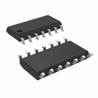
LMC6036IM/NOPB National Semiconductor, LMC6036IM/NOPB Datasheet - Page 14

LMC6036IM/NOPB
Manufacturer Part Number
LMC6036IM/NOPB
Description
IC OP AMP 2.7V SUPP CMOS 14-SOIC
Manufacturer
National Semiconductor
Type
General Purpose Amplifierr
Datasheet
1.LMC6035IBPCONV.pdf
(20 pages)
Specifications of LMC6036IM/NOPB
Amplifier Type
General Purpose
Number Of Circuits
4
Output Type
Rail-to-Rail
Slew Rate
1.5 V/µs
Gain Bandwidth Product
1.4MHz
Current - Input Bias
0.02pA
Voltage - Input Offset
500µV
Current - Supply
1.3mA
Current - Output / Channel
8mA
Voltage - Supply, Single/dual (±)
2 V ~ 15.5 V, ±1 V ~ 7.75 V
Operating Temperature
-40°C ~ 85°C
Mounting Type
Surface Mount
Package / Case
14-SOIC (3.9mm Width), 14-SOL
Rail/rail I/o Type
Rail to Rail Output
Number Of Elements
4
Unity Gain Bandwidth Product
1.4MHz
Common Mode Rejection Ratio
63dB
Input Offset Voltage
5mV
Single Supply Voltage (typ)
3/5/9/12/15V
Dual Supply Voltage (typ)
Not RequiredV
Voltage Gain In Db
126.02dB
Power Supply Rejection Ratio
63dB
Power Supply Requirement
Single
Shut Down Feature
No
Single Supply Voltage (min)
2V
Single Supply Voltage (max)
15.5V
Dual Supply Voltage (min)
Not RequiredV
Dual Supply Voltage (max)
Not RequiredV
Technology
CMOS
Operating Temp Range
-40C to 85C
Operating Temperature Classification
Industrial
Mounting
Surface Mount
Pin Count
14
Package Type
SOIC N
Lead Free Status / RoHS Status
Lead free / RoHS Compliant
-3db Bandwidth
-
Lead Free Status / Rohs Status
Compliant
Other names
*LMC6036IM
*LMC6036IM/NOPB
LMC6036IM
*LMC6036IM/NOPB
LMC6036IM
Available stocks
Company
Part Number
Manufacturer
Quantity
Price
Company:
Part Number:
LMC6036IM/NOPB
Manufacturer:
National Semiconductor
Quantity:
1 973
www.national.com
1.0 Application Notes
1.2.2.1 High-Pass Frequency Scaling Procedure
Choose a standard capacitor value and scale the imped-
ances in the circuit according to the desired cutoff frequency
(300Hz) as follows:
x 2π x (desired cutoff freq.)
Hz = 78.05k
R1 = Z x R1
(Standard value chosen for R1 is 110kΩ )
R2 = Z x R2
(Standard value chosen for R1 is 54.9kΩ )
1.2.3 Dual Amplifier Bandpass Filter
The dual amplifier bandpass (DABP) filter features the ability
to independently adjust f
topologies, the f
The DABP filter also offers both low sensitivity to component
values and high Qs. The following application of Figure 7,
provides a 1kHz center frequency and a Q of 100.
1.2.3.1 DABP Component Selection Procedure
Component selection for the DABP filter is performed as
follows:
1. First choose a center frequency (f
2. Then compute R1 for a desired Q (f
component values that were obtained from the following
computation for a center frequency of 1kHz.
(Chosen standard value is 23.7kΩ )
R1 = Q x R2.
23.7kΩ = 2.37MΩ.
= 1/(2 πf
FIGURE 7. 2 Pole, 1kHz Active, Bandpass Filter
R2 = R3 = 1/(2π x 3kHz x 6.8nF) = 23.4kΩ
(normalized)
(normalized)
c
C)
c
and Q adjustments interact with each other.
Given: f
Choosing a Q of 100,
C = C1 = C2
= 78.05k x (1/0.707) = 110.4kΩ
= 78.05k x (1/1.414) = 55.2kΩ
c
and Q. In most other bandpass
c
= 1kHz and C
= 1 Farad/6.8nF x 2π x 300
c
Z = 1 Farad/C
). Figure 7 represents
(Continued)
c
/BW) as follows:
(chosen)
R1 = 100 x
R2 = R3
= 6.8nF
01283050
(chosen)
14
1.3 PRINTED-CIRCUIT-BOARD LAYOUT
FOR HIGH-IMPEDANCE WORK
It is generally recognized that any circuit which must operate
with
the PC board. If one wishes to take advantage of the
ultra-low bias current of the LMC6035/6, typically
it is essential to have an excellent layout. Fortunately, the
techniques for obtaining low leakages are quite simple. First,
the user must not ignore the surface leakage of the PC
board, even though it may at times appear acceptably low.
Under conditions of high humidity, dust or contamination, the
surface leakage will be appreciable.
To minimize the effect of any surface leakage, lay out a ring
of foil completely surrounding the LMC6035 or LMC6036
inputs and the terminals of capacitors, diodes, conductors,
resistors, relay terminals, etc. connected to the op amp’s
inputs. See Figure 8. To have a significant effect, guard rings
should be placed on both the top and bottom of the PC
board. This PC foil must then be connected to a voltage
which is at the same voltage as the amplifier inputs, since no
leakage current can flow between two points at the same
potential. For example, a PC board trace-to-pad resistance
of 10
tance, could leak 5pA if the trace were a 5V bus adjacent to
the pad of an input. This would cause a 100 times degrada-
tion from the amplifiers actual performance. However, if a
guard ring is held within 5mV of the inputs, then even a
resistance of 10
current, or perhaps a minor (2:1) degradation of the amplifi-
er’s performance. See Figure 9a, b, c for typical connections
of guard rings for standard op amp configurations. If both
inputs are active and at high impedance, the guard can be
tied to ground and still provide some protection; see Figure 9
d.
<
12
1000pA of leakage current requires special layout of
Ω, which is normally considered a very large resis-
FIGURE 8. Example, using the LMC6036
of Guard Ring in P.C. Board Layout
11
Ω would cause only 0.05pA of leakage
01283007
<
0.04pA,


