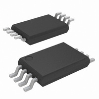
TSC103IPT STMicroelectronics, TSC103IPT Datasheet - Page 10

TSC103IPT
Manufacturer Part Number
TSC103IPT
Description
IC AMP HI SIDE CURR SENSE 8TSSOP
Manufacturer
STMicroelectronics
Specifications of TSC103IPT
Amplifier Type
Current Sense
Number Of Circuits
1
Output Type
Buffered
Slew Rate
0.6 V/µs
-3db Bandwidth
700kHz
Current - Input Bias
10µA
Voltage - Input Offset
500µV
Current - Supply
200µA
Current - Output / Channel
26mA
Voltage - Supply, Single/dual (±)
2.7 V ~ 5.5 V, ±1.35 V ~ 2.75 V
Operating Temperature
-40°C ~ 125°C
Mounting Type
Surface Mount
Package / Case
8-TSSOP
Number Of Channels
Dual
Common Mode Rejection Ratio (min)
90 dB
Input Voltage Range (max)
5.5 V
Input Voltage Range (min)
2.7 V
Input Offset Voltage
1100 uV
Input Bias Current (max)
10 uA
Supply Current
300 uA
Maximum Operating Temperature
+ 125 C
Minimum Operating Temperature
- 40 C
Mounting Style
SMD/SMT
Operating Temperature Range
- 40 C to + 125 C
Supply Voltage (max)
5.5 V
Supply Voltage (min)
2.7 V
No. Of Amplifiers
1
Input Bias Current
15µA
Gain Db Max
100dB
Bandwidth
700kHz
Cmrr
105dB
Supply Voltage Range
2.7V To 5.5V
Rohs Compliant
Yes
Lead Free Status / RoHS Status
Lead free / RoHS Compliant
Gain Bandwidth Product
-
Lead Free Status / Rohs Status
Lead free / RoHS Compliant
Other names
497-10454-2
Available stocks
Company
Part Number
Manufacturer
Quantity
Price
Company:
Part Number:
TSC103IPT
Manufacturer:
CIRRUS
Quantity:
567
Parameter definitions
4
4.1
4.2
4.3
10/23
Parameter definitions
Common mode rejection ratio (CMR)
The common-mode rejection ratio (CMR) measures the ability of the current-sensing
amplifier to reject any DC voltage applied on both inputs V
back to the input so that its effect can be compared with the applied differential signal. The
CMR is defined by the formula:
Supply voltage rejection ratio (SVR)
The supply-voltage rejection ratio (SVR) measures the ability of the current-sensing
amplifier to reject any variation of the supply voltage V
input so that its effect can be compared with the applied differential signal. The SVR is
defined by the formula:
Gain (Av) and input offset voltage (V
The input offset voltage is defined as the intersection between the linear regression of the
V
V
calculated with the following formula.
out
sense
vs. V
= V
sense
sense1
curve with the X-axis (see
and V
V
os
out2
=
SVR
is the output voltage with V
V
CMR
sense1
Doc ID 16873 Rev 1
=
=
–
–
20
–
⎛
⎝
20
V
----------------------------------------------- -
⋅
sense1
V
⋅
log
out1
log
Figure
----------------------------- -
ΔV
------------------------------
ΔV
–
–
ΔV
CC
V
V
ΔV
icm
sense2
out2
out
⋅
4). If V
out
⋅
Av
Av
sense
⋅
CC
os
out1
V
. The SVR is referred back to the
out1
)
p
= V
is the output voltage with
and V
⎞
⎠
sense2
m
. The CMR is referred
, then V
os
can be
TSC103


