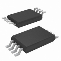
TSC103IPT STMicroelectronics, TSC103IPT Datasheet

TSC103IPT
Specifications of TSC103IPT
Available stocks
Related parts for TSC103IPT
TSC103IPT Summary of contents
Page 1
Features ■ Independent supply and input common-mode voltages ■ Wide common-mode operating range: 2 single-supply configuration -2 dual-supply configuration ■ Wide common-mode surviving range: - (reversed battery and load-dump ...
Page 2
Contents Contents 1 Application schematic and pin description . . . . . . . . . . . . . . . . . . . . . . 3 2 Absolute maximum ratings and operating conditions . . ...
Page 3
TSC103 1 Application schematic and pin description The TSC103 high-side current sense amplifier can be used in either single- or dual-supply mode. In the single-supply configuration, the TSC103 features a wide 2 input common-mode range totally ...
Page 4
Application schematic and pin description Figure 2. Dual-supply configuration schematic 4/23 Vsense Iload Common-mode voltage Rsense Vp Vm Vcc+ Out SEL1 TSC103 SEL2 Vcc- Gnd Doc ID 16873 Rev Vcc µ Controller ...
Page 5
TSC103 Figure 3. Common-mode versus supply voltage in dual-supply configuration common-mode voltage Table 1 describes the function of each pin. Their position is shown in the illustration on the cover page and in Table 1. Pin description Symbol Out Analog ...
Page 6
Absolute maximum ratings and operating conditions 2 Absolute maximum ratings and operating conditions Table 2. Absolute maximum ratings Symbol V Input pins differential voltage ( Sensing pins input voltages (V in_sense V Gain selection pins input voltages (SEL1, ...
Page 7
TSC103 3 Electrical characteristics The electrical characteristics given in the following tables are measured under the following test conditions unless otherwise specified. ● 25° amb ● sense p Table 4. Supply Symbol ...
Page 8
Electrical characteristics Table 6. Output Symbol Parameter Av Gain ΔV /ΔT Output voltage drift vs. T out ΔV /ΔI Output stage load regulation out out ΔV Total output voltage accuracy out ΔV Total output voltage accuracy out ΔV Total output ...
Page 9
TSC103 Table 7. Frequency response Symbol Parameter Response to input differential ts voltage change. Output settling final value Response to a gain change. t SEL Output settling final value Response to common-mode t voltage ...
Page 10
Parameter definitions 4 Parameter definitions 4.1 Common mode rejection ratio (CMR) The common-mode rejection ratio (CMR) measures the ability of the current-sensing amplifier to reject any DC voltage applied on both inputs V back to the input so that its ...
Page 11
TSC103 Figure 4. V out The values of V sense1 Table 9. Table 9. Test conditions for V Av (V/ 100 versus V characteristics: detail for low V sense Vout Vout_1 Vout_2 Vos Vsense2 and V used ...
Page 12
Parameter definitions 4.4 Output voltage drift versus temperature The output voltage drift versus temperature is defined as the maximum variation of V respect to its value at 25° C over the temperature range calculated as follows: with T ...
Page 13
TSC103 4.5 Input offset drift versus temperature The input voltage drift versus temperature is defined as the maximum variation of V respect to its value at 25° C over the temperature range calculated as follows: with T < ...
Page 14
Parameter definitions Figure 7. V out The output voltage accuracy, expressed as a percentage, can be calculated with the following formula, with 20 V/V, 25 V/V, 50 V/V or 100 V/V depending on the configuration of the SEL1 and SEL2 ...
Page 15
TSC103 5 Maximum permissible voltages on pins The TSC103 can be used in either single- or dual-supply configuration. The dual-supply configuration is achieved by disconnecting Vcc- and Gnd, and connecting Vcc negative supply. Figure 8 illustrates how the ...
Page 16
Application information 6 Application information The TSC103 can be used to measure current and to feed back the information to a microcontroller. Figure 9. Single-supply configuration schematic The current from the supply flows to the load through the R drop ...
Page 17
TSC103 The resistor ratio R and to 100 V/V for TSC103C. Since they define the full-scale output range of the application, the resistor ratio (equal to Av) are important parameters and must therefore be selected g3 g1 ...
Page 18
Package information 7 Package information In order to meet environmental requirements, ST offers these devices in different grades of ® ECOPACK packages, depending on their level of environmental compliance. ECOPACK specifications, grade definitions and product status are available at: www.st.com. ...
Page 19
TSC103 7.1 SO-8 package information Figure 10. SO-8 package mechanical drawing Table 10. SO-8 package mechanical data Ref ccc Dimensions Millimeters Min. Typ. Max. 1.75 0.10 0.25 ...
Page 20
Package information 7.2 TSSOP-8 package information Figure 11. TSSOP8 package mechanical drawing Table 11. TSSOP8 package mechanical data Ref aaa 20/23 Dimensions Millimeters Min. Typ. Max. 1.20 0.05 ...
Page 21
... TSC103 8 Ordering information Table 12. Order codes Part number Temperature range TSC103IPT -40° C, +125° C TSC103IDT (1) TSC103IYPT -40° C, +125° C Automotive grade TSC103IYDT 1. Qualification and characterization according to AEC Q100 and Q003 or equivalent, advanced screening according to AEC Q001 & Q002 or equivalent are on-going. ...
Page 22
Revision history 9 Revision history Table 13. Document revision history Date 04-Jan-2010 22/23 Revision 1 Initial release. Doc ID 16873 Rev 1 TSC103 Changes ...
Page 23
... TSC103 Information in this document is provided solely in connection with ST products. STMicroelectronics NV and its subsidiaries (“ST”) reserve the right to make changes, corrections, modifications or improvements, to this document, and the products and services described herein at any time, without notice. All ST products are sold pursuant to ST’s terms and conditions of sale. ...


