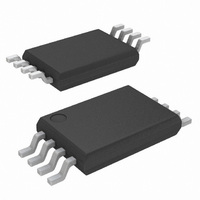
TSC103IPT STMicroelectronics, TSC103IPT Datasheet - Page 13

TSC103IPT
Manufacturer Part Number
TSC103IPT
Description
IC AMP HI SIDE CURR SENSE 8TSSOP
Manufacturer
STMicroelectronics
Specifications of TSC103IPT
Amplifier Type
Current Sense
Number Of Circuits
1
Output Type
Buffered
Slew Rate
0.6 V/µs
-3db Bandwidth
700kHz
Current - Input Bias
10µA
Voltage - Input Offset
500µV
Current - Supply
200µA
Current - Output / Channel
26mA
Voltage - Supply, Single/dual (±)
2.7 V ~ 5.5 V, ±1.35 V ~ 2.75 V
Operating Temperature
-40°C ~ 125°C
Mounting Type
Surface Mount
Package / Case
8-TSSOP
Number Of Channels
Dual
Common Mode Rejection Ratio (min)
90 dB
Input Voltage Range (max)
5.5 V
Input Voltage Range (min)
2.7 V
Input Offset Voltage
1100 uV
Input Bias Current (max)
10 uA
Supply Current
300 uA
Maximum Operating Temperature
+ 125 C
Minimum Operating Temperature
- 40 C
Mounting Style
SMD/SMT
Operating Temperature Range
- 40 C to + 125 C
Supply Voltage (max)
5.5 V
Supply Voltage (min)
2.7 V
No. Of Amplifiers
1
Input Bias Current
15µA
Gain Db Max
100dB
Bandwidth
700kHz
Cmrr
105dB
Supply Voltage Range
2.7V To 5.5V
Rohs Compliant
Yes
Lead Free Status / RoHS Status
Lead free / RoHS Compliant
Gain Bandwidth Product
-
Lead Free Status / Rohs Status
Lead free / RoHS Compliant
Other names
497-10454-2
Available stocks
Company
Part Number
Manufacturer
Quantity
Price
Company:
Part Number:
TSC103IPT
Manufacturer:
CIRRUS
Quantity:
567
TSC1031
4.5
4.6
Input offset drift versus temperature
The input voltage drift versus temperature is defined as the maximum variation of V
respect to its value at 25° C over the temperature range. It is calculated as follows:
with T
Figure 6.
chart V
V
Figure 6.
Output voltage accuracy
The output voltage accuracy is the difference between the actual output voltage and the
theoretical output voltage. Ideally, the current sensing output voltage should be equal to the
input differential voltage multiplied by the theoretical gain, as in the following formula.
The actual value is very slightly different, mainly due to the effects of:
●
●
os
versus T, and T = 25° C is considered to be the reference.
V
the input offset voltage V
the non-linearity.
min
out-th
os
provides a graphical definition of the input offset drift versus temperature. On this
is always comprised in the area defined by the maximum and minimum variation of
< T
= Av . V
amb
Input offset drift versus temperature (Av = 50 V/V)
< T
-0.5
-1.5
-2.5
sense
1.5
0.5
max
-1
-2
1
0
-60 -40 -20
.
ΔV os
-------------- -
ΔT
os
=
Doc ID 16875 Rev 1
,
max
V os T amb
---------------------------------------------------------------------
0
(
T amb 25° C
20
) V os 25° C
T (°C)
–
–
40
(
60
80 100 120 140
)
Parameter definitions
os
with
13/23


