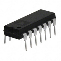
AD704JNZ Analog Devices Inc, AD704JNZ Datasheet - Page 7

AD704JNZ
Manufacturer Part Number
AD704JNZ
Description
IC OPAMP GP QUAD PREC LN 14DIP
Manufacturer
Analog Devices Inc
Specifications of AD704JNZ
Slew Rate
0.15 V/µs
Amplifier Type
General Purpose
Number Of Circuits
4
-3db Bandwidth
800kHz
Current - Input Bias
100pA
Voltage - Input Offset
50µV
Current - Supply
1.5mA
Current - Output / Channel
15mA
Voltage - Supply, Single/dual (±)
4 V ~ 36 V, ±2 V ~ 18 V
Operating Temperature
0°C ~ 70°C
Mounting Type
Through Hole
Package / Case
14-DIP (0.300", 7.62mm)
Op Amp Type
Precision
No. Of Amplifiers
4
Bandwidth
800kHz
Supply Voltage Range
± 2V To ± 18V
Amplifier Case Style
DIP
No. Of Pins
14
Common Mode Rejection Ratio
100
Current, Input Bias
270 pA
Current, Input Offset
1 pA
Current, Supply
600 μA
Number Of Amplifiers
Quad
Package Type
PDIP-14
Power Dissipation
650 mW
Temperature, Operating, Range
-55 to +125 °C
Voltage, Gain
200 V/mV
Voltage, Input
±18 V
Voltage, Noise
15 nV/sqrt Hz
Voltage, Offset
150 μV
Voltage, Output, High
+13 V
Voltage, Output, Low
-13 V
Voltage, Supply
±18 V
Lead Free Status / RoHS Status
Lead free / RoHS Compliant
Output Type
-
Gain Bandwidth Product
-
Lead Free Status / Rohs Status
RoHS Compliant part
Electrostatic Device
120
100
Figure 14. Change in Input Offset Voltage vs. Warm-Up Time
80
60
40
20
50
40
30
20
10
4
3
2
1
0
Figure 13. Typical Distribution of Input Offset Voltage Drift
0
–15
0
Figure 15. Input Bias Current vs. Common-Mode Voltage
0
–0.8
–10
INPUT OFFSET VOLTAGE DRIFT (µV/°C)
1
COMMON-MODE VOLTAGE (V)
–0.4
WARM-UP TIME (Minutes)
–5
2
NEGATIVE I
POSITIVE I
0
0
B
B
3
5
0.4
4
10
0.8
15
5
Rev. E | Page 7 of 16
0.5µV
100
100
1k
10
1k
10
1
1
1
1
0
Figure 16. Input Noise Voltage Spectral Density
Figure 17. Input Noise Current Spectral Density
Figure 18. 0.1 Hz to 10 Hz Noise Voltage
100Ω
20MΩ
10kΩ
10
10
FREQUENCY (Hz)
FREQUENCY (Hz)
TIME (Seconds)
5
V
OUT
100
100
AD704
1k
1k
10


