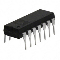
AD704JNZ Analog Devices Inc, AD704JNZ Datasheet - Page 11

AD704JNZ
Manufacturer Part Number
AD704JNZ
Description
IC OPAMP GP QUAD PREC LN 14DIP
Manufacturer
Analog Devices Inc
Specifications of AD704JNZ
Slew Rate
0.15 V/µs
Amplifier Type
General Purpose
Number Of Circuits
4
-3db Bandwidth
800kHz
Current - Input Bias
100pA
Voltage - Input Offset
50µV
Current - Supply
1.5mA
Current - Output / Channel
15mA
Voltage - Supply, Single/dual (±)
4 V ~ 36 V, ±2 V ~ 18 V
Operating Temperature
0°C ~ 70°C
Mounting Type
Through Hole
Package / Case
14-DIP (0.300", 7.62mm)
Op Amp Type
Precision
No. Of Amplifiers
4
Bandwidth
800kHz
Supply Voltage Range
± 2V To ± 18V
Amplifier Case Style
DIP
No. Of Pins
14
Common Mode Rejection Ratio
100
Current, Input Bias
270 pA
Current, Input Offset
1 pA
Current, Supply
600 μA
Number Of Amplifiers
Quad
Package Type
PDIP-14
Power Dissipation
650 mW
Temperature, Operating, Range
-55 to +125 °C
Voltage, Gain
200 V/mV
Voltage, Input
±18 V
Voltage, Noise
15 nV/sqrt Hz
Voltage, Offset
150 μV
Voltage, Output, High
+13 V
Voltage, Output, Low
-13 V
Voltage, Supply
±18 V
Lead Free Status / RoHS Status
Lead free / RoHS Compliant
Output Type
-
Gain Bandwidth Product
-
Lead Free Status / Rohs Status
RoHS Compliant part
Electrostatic Device
THEORY OF OPERATION
The instrumentation amplifier with post filtering (see Figure 34)
combines two applications that benefit greatly from the AD704.
This circuit achieves low power and dc precision over temperature
with a minimum of components.
The instrumentation amplifier circuit offers many performance
benefits, including BiFET level input bias currents, low input
offset voltage drift, and only 1.2 mA quiescent current. It operates
for gains that are G ≥ 2 and, at lower gains, it benefits from no
output amplifier offset and no noise contribution as encountered
in a 3-op-amp design. Good low frequency CMRR is achieved
even without the optional ac CMRR trim (see Figure 35). Table 4
provides resistance values for three common circuit gains. For
other gains, use the following equations:
Table 4. Resistance Values for Various Gains
Circuit
Gain (G)
10
100
1000
C
R2
R1
Max
(5kΩ POT)
NOTES
1. INSTRUMENTATION AMPLIFIER GAIN = 1 +
2. CAPACITORS C2 AND C4 ARE SOUTHERN ELECTRONICS MPCC, POLYCARBONATE, ±5%, 50V.
3. ALL RESISTORS METAL FILM, 1%.
2.4kΩ
–V
+V
R5
CMRR
t
TRIM
IN
IN
AC CMRR TRIM
DC
≈
=
=
OPTIONAL
Value
π 2
R3
R4
47.5kΩ
R1 and R3
6.34 kΩ
526 Ω
56.2 Ω
R4
(
=
+
R3
0
R5
49
of
9 .
1
)
5
C
9 .
=
R
G
t
×
G
k
49
10
−
Ω
=
AD704
1
9 .
5
R
Trim Potentiometer)
166 kΩ
16.6 kΩ
1.66 kΩ
1/4
99
+V
6.34kΩ
. 0
G
k
(Max Value of
R3
S
Ω
8 .
06
(500kΩ POT)
GAIN TRIM
0.1µF
k
G
Ω
R
G
6.34kΩ
R2
R1
Figure 34. Gain-of-10 Instrumentation Amplifier with Post Filtering
R1
+
2R2
R
G
(FOR R1 = R3, R2 = R4 + R5).
AD704
Bandwidth
(−3 dB), Hz
50 k
5k
0.5 k
1/4
49.9kΩ
–V
R2
S
0.1µF
Rev. E | Page 11 of 16
OPTIONAL BALANCE RESISTOR NETWORKS
1MΩ
R6
CAN BE REPLACED WITH A SHORT.
1MΩ
R7
Q
ω =
R6 = R7
1
=
C2
R6 C1C2
Figure 35. Common-Mode Rejection vs. Frequency with and Without
C1
4C2
C1
160
140
120
100
1
80
60
40
20
AD704
C5, 0.01µF
0
R10, 2MΩ
1
1/4
TYPICAL MONOLITHIC IN AMP
GAIN = 10, 0.2V p-p COMMON-MODE INPUT
1MΩ
10
R8
1MΩ
FREQUENCY (Hz)
WITHOUT CAPACITOR C
R9
Capacitor C
Q
ω =
R8 = R9
2
100
=
R8 C3C4
C4
C3
4C4
C3
1
t
AD704
C6, 0.01µF
R11, 2MΩ
CIRCUIT TRIMMED
USING CAPACITOR C
1/4
1k
t
OUTPUT
AD704
t
10k


