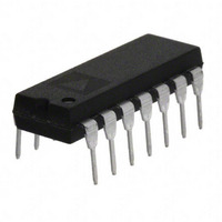
AD704JNZ Analog Devices Inc, AD704JNZ Datasheet - Page 5

AD704JNZ
Manufacturer Part Number
AD704JNZ
Description
IC OPAMP GP QUAD PREC LN 14DIP
Manufacturer
Analog Devices Inc
Specifications of AD704JNZ
Slew Rate
0.15 V/µs
Amplifier Type
General Purpose
Number Of Circuits
4
-3db Bandwidth
800kHz
Current - Input Bias
100pA
Voltage - Input Offset
50µV
Current - Supply
1.5mA
Current - Output / Channel
15mA
Voltage - Supply, Single/dual (±)
4 V ~ 36 V, ±2 V ~ 18 V
Operating Temperature
0°C ~ 70°C
Mounting Type
Through Hole
Package / Case
14-DIP (0.300", 7.62mm)
Op Amp Type
Precision
No. Of Amplifiers
4
Bandwidth
800kHz
Supply Voltage Range
± 2V To ± 18V
Amplifier Case Style
DIP
No. Of Pins
14
Common Mode Rejection Ratio
100
Current, Input Bias
270 pA
Current, Input Offset
1 pA
Current, Supply
600 μA
Number Of Amplifiers
Quad
Package Type
PDIP-14
Power Dissipation
650 mW
Temperature, Operating, Range
-55 to +125 °C
Voltage, Gain
200 V/mV
Voltage, Input
±18 V
Voltage, Noise
15 nV/sqrt Hz
Voltage, Offset
150 μV
Voltage, Output, High
+13 V
Voltage, Output, Low
-13 V
Voltage, Supply
±18 V
Lead Free Status / RoHS Status
Lead free / RoHS Compliant
Output Type
-
Gain Bandwidth Product
-
Lead Free Status / Rohs Status
RoHS Compliant part
Electrostatic Device
ABSOLUTE MAXIMUM RATINGS
Table 3.
Parameter
Supply Voltage
Internal Power Dissipation (25°C)
Input Voltage
Differential Input Voltage
Output Short-Circuit Duration (Single Input)
Storage Temperature Range
Operating Temperature Range
Lead Temperature (Soldering, 10 sec)
1
2
Stresses above those listed under Absolute Maximum Ratings
may cause permanent damage to the device. This is a stress
rating only; functional operation of the device at these or any
other conditions above those indicated in the operational
section of this specification is not implied. Exposure to absolute
maximum rating conditions for extended periods may affect
device reliability.
INPUT SIGNAL
NOTES
1. ALL FOUR AMPLIFIERS ARE CONNECTED AS SHOWN.
1
THE SIGNAL INPUT (SUCH THAT THE AMPLIFIER’S OUTPUT IS AT MAXIMUM
Specification is for the device in free air:
The input pins of this amplifier are protected by back-to-back diodes. If the
differential voltage exceeds ±0.7 volts, external series protection resistors
should be added to limit the input current to less than 25 mA.
AMPLITUDE WITHOUT CLIPPING OR SLEW LIMITING) IS APPLIED TO ONE
AMPLIFIER AT A TIME. THE OUTPUTS OF THE OTHER THREE AMPLIFIERS ARE
THEN MEASURED FOR CROSSTALK.
AD704J
AD704A
14-lead plastic package: θ
16-lead SOIC package: θ
20-terminal LCC package: θ
1kΩ
1
1kΩ
AD704
Figure 5. Crosstalk Test Circuit
1/4
9kΩ
JA
JA
= 100°C/W.
2
JA
= 150°C/W.
= 150°C/W.
2.5kΩ
OUTPUT
1
COM
+V
–V
S
S
0.1µF
0.1µF
Rating
±18 V
±V
±0.7 V
Indefinite
−65°C to +125°C
0°C to 70°C
−40°C to +85°C
300°C
1µF
1µF
S
AD704
PIN 4
AD704
PIN 11
Rev. E | Page 5 of 16
ESD CAUTION
–100
–120
–140
–160
–80
10
Figure 6. Crosstalk vs. Frequency
100
FREQUENCY (Hz)
1k
10k
AMP4
AMP2
AMP3
AD704
100k


