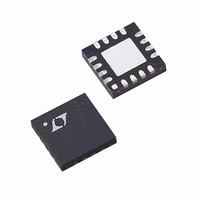
LTC6404IUD-2#PBF Linear Technology, LTC6404IUD-2#PBF Datasheet - Page 8

LTC6404IUD-2#PBF
Manufacturer Part Number
LTC6404IUD-2#PBF
Description
IC AMP/DRIVER DIFF 16-QFN
Manufacturer
Linear Technology
Type
ADC Driverr
Specifications of LTC6404IUD-2#PBF
Applications
Data Acquisition
Mounting Type
Surface Mount
Package / Case
16-WQFN Exposed Pad
Current - Supply
30.4mA
Operating Temperature
-40°C ~ 85°C
Output Type
Differential, Rail-to-Rail
Number Of Circuits
1
Current - Output / Channel
85mA
Amplifier Type
Differential
Voltage - Supply, Single/dual (±)
2.7 V ~ 5.5 V, ±1.35 V ~ 2.75 V
-3db Bandwidth
600MHz
Slew Rate
700 V/µs
Gain Bandwidth Product
900MHz
Current - Input Bias
23µA
Voltage - Input Offset
500µV
Number Of Channels
1
Number Of Elements
1
Power Supply Requirement
Single
Common Mode Rejection Ratio
60dB
Voltage Gain Db
90dB
Unity Gain Bandwidth Product (typ)
900MHz
Input Resistance
1@3V@-40C TO 85CMohm
Single Supply Voltage (typ)
3/5V
Dual Supply Voltage (typ)
Not RequiredV
Power Supply Rejection Ratio
60dB
Rail/rail I/o Type
Rail to Rail Output
Single Supply Voltage (min)
2.7V
Single Supply Voltage (max)
5.25V
Dual Supply Voltage (min)
Not RequiredV
Dual Supply Voltage (max)
Not RequiredV
Operating Temp Range
-40C to 85C
Operating Temperature Classification
Industrial
Mounting
Surface Mount
Pin Count
16
Package Type
QFN EP
No. Of Amplifiers
1
Input Offset Voltage
2mV
Gain Db Max
2dB
Bandwidth
900MHz
Supply Voltage Range
2.7V To 5.25V
Supply Current
30.4mA
Amplifier Case Style
QFN
Rohs Compliant
Yes
Lead Free Status / RoHS Status
Lead free / RoHS Compliant
Available stocks
Company
Part Number
Manufacturer
Quantity
Price
LTC6404-2
TYPICAL PERFORMANCE CHARACTERISTICS
PIN FUNCTIONS
SHDN (Pin 1): When SHDN is fl oating or directly tied to V
the LTC6404-2 is in the normal (active) operating mode.
When Pin 1 is pulled a minimum of 2.1V below V
LTC6404-2 enters into a low power shutdown state. See
Applications Information for more details.
V
Pins. Three pairs of power supply pins are provided to keep
the power supply inductance as low as possible to prevent
degradation of amplifi er 2nd harmonic performance. See
the Layout Considerations section for more detail.
8
+
, V
–
(Pins 2, 10, 11 and Pins 3, 9, 12): Power Supply
–100
–110
–120
–100
–120
–40
–50
–60
–70
–80
–90
–20
–40
–60
–80
0
0
Distortion vs Output Amplitude
LTC6404-2 Driving LTC2207
16-Bit ADC (Two Tones)
0
V
V
R
V
IM3L
f
IN
S
CM
I
IN
= 100Ω, R
= 3V
= SINGLE-ENDED INPUT
= 10MHz
= V
HD2
1
10
OCM
HD3
IM3U
= MID-SUPPLY
F
FREQUENCY (MHz)
2
= 200Ω
V
OUTDIFF
20
V
V
FULLY-DIFFERENTIAL
V
V
R
16184 POINT FFT
f
TONE1, TONE2 = –7dBFS
IM3U= –106.8dBc
IM3L= –107.7dBc
SAMPLE
S
INDIFF
OUTDIFF
CM
I
3
= 100Ω, R
= 3.3V
(V
= V
30
P-P
= 1V
OCM
= 105Msps
= 2V
)
4
P-P
= 1.25V
F
P-P
40
= 200Ω
5
64042 G19
64042 G21
50
6
+
, the
+
,
V
The voltage on the V
mode voltage level (which is defi ned as the average of the
voltages on the OUT
midpoint of an internal resistive voltage divider between
the supplies, developing a (default) mid-supply voltage
potential to maximize output signal swing. In general,
the V
source/reference capable of driving the input impedance
presented by the V
OCM
OCM
(Pin 4): Output Common Mode Reference Voltage.
–100
–120
–20
–40
–60
–80
100
10
0
0.01
1
0
LTC6404-2 Driving LTC2207
16-Bit ADC (Single Tone)
Voltage Noise Density vs
Frequency
pin can be over-driven by an external voltage
V
V
R
T
A
S
CM
I
= 100Ω, R
= 25°C
= 3V
= V
10
0.1
OCM
DIFFERENTIAL INPUT
REFERRED
COMMON MODE
FREQUENCY (MHz)
OCM
= MID-SUPPLY
F
FREQUENCY (MHz)
+
HD2
= 200Ω
20
and OUT
1
OCM
V
V
V
R
10.1MHz, 16184 POINT FFT
f
FUNDAMENTAL = –1dBFS
HD2 = –92.4dBc
HD3 = –93.02dBc
SAMPLE
S
OUTDIFF
CM
I
pin. On the LTC6404-2, the V
= 100Ω, R
= 3.3V
= V
HD3
30
pin sets the output common
10
OCM
= 105Msps
HD7
= 2V
–
= 1.25V
F
P-P
pins). The V
= 200Ω
HD4
40
100
64042 G20
64042 G22
HD5
50
1000
OCM
pin is the
64042f
OCM


