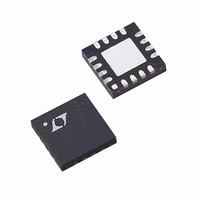
LTC6404IUD-2#PBF Linear Technology, LTC6404IUD-2#PBF Datasheet - Page 3

LTC6404IUD-2#PBF
Manufacturer Part Number
LTC6404IUD-2#PBF
Description
IC AMP/DRIVER DIFF 16-QFN
Manufacturer
Linear Technology
Type
ADC Driverr
Specifications of LTC6404IUD-2#PBF
Applications
Data Acquisition
Mounting Type
Surface Mount
Package / Case
16-WQFN Exposed Pad
Current - Supply
30.4mA
Operating Temperature
-40°C ~ 85°C
Output Type
Differential, Rail-to-Rail
Number Of Circuits
1
Current - Output / Channel
85mA
Amplifier Type
Differential
Voltage - Supply, Single/dual (±)
2.7 V ~ 5.5 V, ±1.35 V ~ 2.75 V
-3db Bandwidth
600MHz
Slew Rate
700 V/µs
Gain Bandwidth Product
900MHz
Current - Input Bias
23µA
Voltage - Input Offset
500µV
Number Of Channels
1
Number Of Elements
1
Power Supply Requirement
Single
Common Mode Rejection Ratio
60dB
Voltage Gain Db
90dB
Unity Gain Bandwidth Product (typ)
900MHz
Input Resistance
1@3V@-40C TO 85CMohm
Single Supply Voltage (typ)
3/5V
Dual Supply Voltage (typ)
Not RequiredV
Power Supply Rejection Ratio
60dB
Rail/rail I/o Type
Rail to Rail Output
Single Supply Voltage (min)
2.7V
Single Supply Voltage (max)
5.25V
Dual Supply Voltage (min)
Not RequiredV
Dual Supply Voltage (max)
Not RequiredV
Operating Temp Range
-40C to 85C
Operating Temperature Classification
Industrial
Mounting
Surface Mount
Pin Count
16
Package Type
QFN EP
No. Of Amplifiers
1
Input Offset Voltage
2mV
Gain Db Max
2dB
Bandwidth
900MHz
Supply Voltage Range
2.7V To 5.25V
Supply Current
30.4mA
Amplifier Case Style
QFN
Rohs Compliant
Yes
Lead Free Status / RoHS Status
Lead free / RoHS Compliant
Available stocks
Company
Part Number
Manufacturer
Quantity
Price
LTC6404-2 DC ELECTRICAL CHARACTERISTICS
over the full operating temperature range, otherwise specifi cations are at T
V
V
SYMBOL
V
ΔV
I
ΔI
I
R
C
e
i
e
V
(Note 7)
CMRRI
(Note 8)
CMRRIO
(Note 8)
PSRR
(Note 9)
PSRRCM
(Note 9)
G
BAL
V
ΔV
V
(Note 7)
R
V
V
n
B
OS
n
nVOCM
SHDN
OUTCM
OSDIFF
IN
ICMR
OSCM
OUTCMR
MID
OUT
IN
CM
INVOCM
B
OSDIFF
OSCM
/ΔT
= OPEN, R
/ΔT
/ΔT Differential Offset Voltage Drift (Input Referred)
= (V
OUT
PARAMETER
Differential Offset Voltage (Input Referred)
Input Bias Current (Note 6)
Input Bias Current Drift (Note 6)
Input Offset Current (Note 6)
Input Resistance
Input Capacitance
Differential Input Referred Noise Voltage Density
Input Noise Current Density
Input Referred Common Mode Noise Voltage
Density
Input Signal Common Mode Range
Input Common Mode Rejection Ratio
(Input Referred) ΔV
Output Common Mode Rejection Ratio (Input
Referred) ΔV
Differential Power Supply Rejection
(ΔV
Output Common Mode Power Supply Rejection
(ΔV
Common Mode Gain (ΔV
Common Mode Gain Error
Output Balance (ΔV
Common Mode Offset Voltage (V
Common Mode Offset Voltage Drift
Output Signal Common Mode Range
(Voltage Range for the V
Input Resistance, V
Voltage at the V
Output Voltage, High, Either Output Pin (Note 10)
Output Voltage, Low, Either Output Pin (Note 10)
+
S
S
+ V
I
/ΔV
/ΔV
= 100Ω, R
OUT
OSDIFF
OSCM
–
OCM
)/2. V
)
)
OCM
/ΔV
F
= 200Ω, R
ICM
OCM
OUTCM
ICM
Pin
OSDIFF
/ΔV
is defi ned as (V
Pin
OCM
OUTCM
/ΔV
OSDIFF
Pin)
OUTDIFF
/ΔV
L
OUTCM
= OPEN, R
OCM
)
)
– V
IN
OCM
+
BAL
+ V
)
IN
= 100kΩ (See Figure 1) unless otherwise noted. V
–
)/2. V
CONDITIONS
V
V
V
V
V
Common Mode
Differential Mode
f = 1MHz
f = 1MHz
f = 1MHz, Referred to V
V
V
V
V
V
V
V
V
V
ΔV
Single-Ended Input
Differential Input
V
V
V
V
V
V
V
V
V
V
V
V
V
V
V
V
V
S
S
S
S
S
S
S
S
S
S
S
S
S
S
S
S
S
S
S
S
S
S
S
S
S
S
S
S
S
S
S
OUTDIFF
= 2.7V to 5.25V
= 2.7V to 5.25V
= 2.7V to 5.25V
= 2.7V to 5.25V
= 2.7V to 5.25V
= 3V
= 5V
= 3V, ΔV
= 5V, ΔV
= 5V, ΔV
= 2.7V to 5.25V
= 2.7V to 5.25V
= 5V, ΔV
= 5V, ΔV
= 2.7V to 5.25V
= 2.7V to 5.25V
= 3V
= 5V
= 3V
= 3V, I
= 3V, I
= 3V, I
= 5V, I
= 5V, I
= 5V, I
= 3V, I
= 3V, I
= 3V, I
= 5V, I
= 5V, I
= 5V, I
OUTDIFF
L
L
L
L
L
L
L
L
L
L
L
L
= 2V
= 0
= –5mA
= –20mA
= 0
= –5mA
= –20mA
= 0
= 5mA
= 20mA
= 0
= 5mA
= 20mA
ICM
ICM
OCM
OCM
OCM
is defi ned as (V
= 0.75V
= 1.25V
= 1V
= 1V
= 1V
A
= 25°C. V
OCM
Pin
+
The
OUT
= 3V, V
+
l
– V
denotes the specifi cations which apply
–
OUT
l
l
l
l
l
l
l
l
l
l
l
l
l
l
l
l
l
l
l
l
l
l
l
l
l
l
l
l
l
= 0V, V
–
). V
–0.6
1.45
MIN
–60
1.1
1.1
60
50
CM
0
0
8
INDIFF
= V
S
is defi ned as (V
= (V
OCM
–0.25
1000
LTC6404-2
±0.5
0.01
10.5
TYP
–23
–60
–66
±10
325
360
480
460
500
650
120
140
200
175
200
285
1.5
1.5
±1
60
60
66
94
63
20
14
1
3
1
3
1
INP
= V
– V
ICM
INM
MAX
1000
1.55
±10
–40
–40
±50
550
600
750
700
750
230
260
350
320
350
550
= Mid-Supply,
1.6
3.6
0.1
±2
20
0
2
4
+
).
– V
–
nV/√Hz
pA/√Hz
nV/√Hz
).
UNITS
μV/°C
μA/°C
μV/°C
64042f
3
V/V
mV
mV
mV
mV
mV
mV
mV
mV
mV
mV
mV
mV
mV
mV
kΩ
kΩ
kΩ
μA
μA
dB
dB
dB
dB
dB
dB
dB
pF
%
V
V
V
V
V


