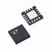
LTC6404IUD-2#PBF Linear Technology, LTC6404IUD-2#PBF Datasheet - Page 12

LTC6404IUD-2#PBF
Manufacturer Part Number
LTC6404IUD-2#PBF
Description
IC AMP/DRIVER DIFF 16-QFN
Manufacturer
Linear Technology
Type
ADC Driverr
Specifications of LTC6404IUD-2#PBF
Applications
Data Acquisition
Mounting Type
Surface Mount
Package / Case
16-WQFN Exposed Pad
Current - Supply
30.4mA
Operating Temperature
-40°C ~ 85°C
Output Type
Differential, Rail-to-Rail
Number Of Circuits
1
Current - Output / Channel
85mA
Amplifier Type
Differential
Voltage - Supply, Single/dual (±)
2.7 V ~ 5.5 V, ±1.35 V ~ 2.75 V
-3db Bandwidth
600MHz
Slew Rate
700 V/µs
Gain Bandwidth Product
900MHz
Current - Input Bias
23µA
Voltage - Input Offset
500µV
Number Of Channels
1
Number Of Elements
1
Power Supply Requirement
Single
Common Mode Rejection Ratio
60dB
Voltage Gain Db
90dB
Unity Gain Bandwidth Product (typ)
900MHz
Input Resistance
1@3V@-40C TO 85CMohm
Single Supply Voltage (typ)
3/5V
Dual Supply Voltage (typ)
Not RequiredV
Power Supply Rejection Ratio
60dB
Rail/rail I/o Type
Rail to Rail Output
Single Supply Voltage (min)
2.7V
Single Supply Voltage (max)
5.25V
Dual Supply Voltage (min)
Not RequiredV
Dual Supply Voltage (max)
Not RequiredV
Operating Temp Range
-40C to 85C
Operating Temperature Classification
Industrial
Mounting
Surface Mount
Pin Count
16
Package Type
QFN EP
No. Of Amplifiers
1
Input Offset Voltage
2mV
Gain Db Max
2dB
Bandwidth
900MHz
Supply Voltage Range
2.7V To 5.25V
Supply Current
30.4mA
Amplifier Case Style
QFN
Rohs Compliant
Yes
Lead Free Status / RoHS Status
Lead free / RoHS Compliant
Available stocks
Company
Part Number
Manufacturer
Quantity
Price
APPLICATIONS INFORMATION
LTC6404-2
appear as open collectors with a non-linear capacitor in
parallel and steering diodes to either supply. Because of
the non-linear capacitance, the outputs still have the ability
to sink and source small amounts of transient current if
driven by signifi cant voltage transients. The inputs (IN
and IN
if voltage transients at the input exceed 1.4V. The inputs
also have steering diodes to either supply. The turn-on and
turn-off time between the shutdown and active states is
typically less than 1μs.
General Amplifi er Applications
As levels of integration have increased and correspond-
ingly, system supply voltages decreased, there has been
a need for ADCs to process signals differentially in order
to maintain good signal to noise ratios. These ADCs are
typically supplied from a single supply voltage which can
be as low as 3V (2.7V min), and will have an optimal com-
mon mode input range near mid-supply. The LTC6404-2
makes interfacing to these ADCs easy by providing both
single ended to differential conversion as well as common
mode level shifting. The front page of this datasheet shows
shows a typical application.
Referring to Figure 1, the gain to V
V
Note from the above equation, the differential output volt-
age (VOUT
and output common mode voltages, or the voltage at the
common mode pin. This makes the LTC6404-2 ideally
suited for pre-amplifi cation, level shifting and conversion
of single ended signals to differential output signals to
drive differential input ADCs.
Effects of Resistor Pair Mismatch
In the circuit of Figure 3, it is possible the gain setting
resistors will not perfectly match. Assuming infi nite open
loop gain, the differential output relationship is given by
the equation:
12
INP
V
OUTDIFF
is:
–
) appear as anti-parallel diodes which can conduct
+
= V
– VOUT
OUT
+
–
) is completely independent of input
– V
OUT
–
R
R
F
I
OUTDIFF
• V
(
INP
from V
– V
INM
INM
)
and
+
,
where:
R
of R
β
from the outputs to their respective inputs:
Δβ is defi ned as the difference in feedback factors:
V
V
mon mode voltage):
and V
voltages:
V
V
INM
AVG
INCM
INP
INP
F
V
V
V
is the average of R
+
–
+
–
, and V
INDIFF
I1
INCM
OUTDIFF
AVG
AVG
V
is defi ned as the average feedback factor (or gain)
V
, and R
VOCM
0.01μF
SHDN
INDIFF
is defi ned as the average of the two input voltages
=
0.1μF
V
V
+
–
R
=
• V
=
= V
Figure 3. Basic Differential Amplifi er with
Feedback Resistor Pair Mismatch
I2
INM
2
1
2
R
1
INCM
= V
+ R
I2
•
is defi ned as the difference of the input
I2
1
2
3
4
INP
• V
SHDN
V
V
V
(also called the source-referred input com-
.
+
–
OCM
(
OUT
R
F2
R
R
16
V
V
I2
I1
5
SHDN
INP
– V
+
–
–
I1
NC
NC
R
–
+ R
+
V
V
I1
INM
IN
IN
+ V
AVG
R
– V
+
–
15
6
F1
I1
F1
R
IN
IN
INM
+ R
, and R
OUT
+
–
V
+
–
R
R
• V
+
I1
OCM
F2
F1
R
F1
)
OCM
–
I2
14
7
R
OUT
OUT
+ R
F2
I2
R
R
–
+
V
V
F
, and R
I
OUTF
OUTF
F2
13
8
• V
–
+
OUTF
OUTF
LTC6404-2
V
INDIFF
+
–
+
V
V
–
–
64042 F03
I
V
V
V
V
–
+
+
–
is the average
12
11
10
9
+
V
V
OUT
OUT
0.1μF
0.1μF
–
+
0.1μF
0.1μF
0.1μF
64042f
V
V
V
+
–
–


