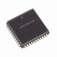
DS89C420-QCL Maxim Integrated Products, DS89C420-QCL Datasheet - Page 23

DS89C420-QCL
Manufacturer Part Number
DS89C420-QCL
Description
IC MCU ULTRA 33MHZ HP 44-PLCC
Manufacturer
Maxim Integrated Products
Series
89Cr
Datasheet
1.DS89C420-QCS.pdf
(47 pages)
Specifications of DS89C420-QCL
Core Processor
8051
Core Size
8-Bit
Speed
33MHz
Connectivity
EBI/EMI, SIO, UART/USART
Peripherals
Power-Fail Reset, WDT
Number Of I /o
32
Program Memory Size
16KB (16K x 8)
Program Memory Type
FLASH
Ram Size
1K x 8
Voltage - Supply (vcc/vdd)
4.5 V ~ 5.5 V
Oscillator Type
External
Operating Temperature
0°C ~ 70°C
Package / Case
44-LCC, 44-PLCC
Lead Free Status / RoHS Status
Contains lead / RoHS non-compliant
Eeprom Size
-
Data Converters
-
Available stocks
Company
Part Number
Manufacturer
Quantity
Price
Company:
Part Number:
DS89C420-QCL
Manufacturer:
PHI
Quantity:
6 217
Company:
Part Number:
DS89C420-QCL
Manufacturer:
Maxim Integrated
Quantity:
10 000
Figure 7. Interfacing the Bootloader to a PC
PARALLEL PROGRAMMING
The DS89C420 allows parallel programming of its internal flash memory compatible with standard flash or EPROM
programmers. In parallel programming mode, a mass-erase command is used to erase all memory locations in the
16kB program memory, the security block, and the memory bank select. Erasing the memory bank select sets it to
the default state; the memory bank select cannot be altered otherwise. If lock bit LB2 has not been programmed,
the program code can be read back for verification. The state of the lock bits can also be verified directly in the
parallel programming mode. One instruction is used to read signature information (at addresses 30, 31, and 60h).
Separate instructions are used for the option control register.
The following sequence can be used to program the flash memory in the parallel programming mode:
1) The DS89C420 is powered up and running at a clock speed between 4MHz and 6MHz.
2) Set RST = EA = 1 and PSEN = 0.
3) Apply the appropriate logic combination to pins P2.6, P2.7, P3.6, and P3.7 to select one of the flash
4) Pulse ALE/ PROG once to perform an erase/program operation.
5) Repeat steps 3 and 4 as necessary.
ON-CHIP MOVX DATA MEMORY
On-chip data memory is provided by the 1kB SRAM and occupies addresses 0000h through 03FFh. The internal
data memory is disabled after a power-on reset, and any MOVX instruction directs the data memory access to the
external data memory. To enable the internal data memory, software must configure the data memory enable bits
DME1 and DME0 (PMR.1-0). See “SFR Bit Descriptions” in the Ultra-High-Speed Flash Microcontroller User’s
Guide for data memory configurations. Once enabled, MOVX instructions with addresses inside the 1k range
access the on-chip data memory, and addresses exceeding the 1k range automatically access external data
memory.
An internal data memory cycle spans only one system clock period to support fast internal execution.
instructions shown in
For program operation, apply the desired address to pins P1.7:0 and P2.5:0. Data is written to port 0.
For verify operation, apply the desired address to pins P1.7:0 and P2.5:0. Data is read at port 0.
Table
7.
23 of 47


