R8A77850ADBGV Renesas Electronics America, R8A77850ADBGV Datasheet - Page 853
R8A77850ADBGV
Manufacturer Part Number
R8A77850ADBGV
Description
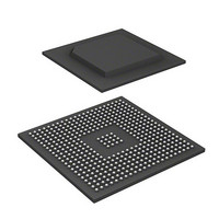
IC SUPERH MPU ROMLESS 436-BGA
Manufacturer
Renesas Electronics America
Series
SuperH® SH7780r
Datasheet
1.R8A77850AADBGV.pdf
(1694 pages)
Specifications of R8A77850ADBGV
Core Processor
SH-4A
Core Size
32-Bit
Speed
600MHz
Connectivity
Audio Codec, MMC, Serial Sound, SCI, SIO, SPI, SSI
Peripherals
DMA, POR, WDT
Number Of I /o
108
Program Memory Type
ROMless
Ram Size
8K x 8
Voltage - Supply (vcc/vdd)
1 V ~ 1.2 V
Oscillator Type
External
Operating Temperature
-40°C ~ 85°C
Package / Case
436-BGA
Lead Free Status / RoHS Status
Lead free / RoHS Compliant
Eeprom Size
-
Program Memory Size
-
Data Converters
-
Available stocks
Company
Part Number
Manufacturer
Quantity
Price
Company:

Part Number:
R8A77850ADBGV
Manufacturer:
Renesas Electronics America
Quantity:
10 000
Company:
Part Number:
R8A77850ADBGV#RD0Z
Manufacturer:
Renesas Electronics America
Quantity:
10 000


Note: In this section, unless otherwise noted, "dot clock" refers to the output dot clock.
19.3
Register update methods include external update and internal update.
(1)
An "external update" is an update which reflects the address-mapped register settings made by the
CPU after the end of CPU access. Registers related to display control (for example, the display
system control register) and the settings of which are updated through external updates can be
overwritten during the vertical blanking interval without display flicker by using the VBK flag and
FRM flag in the display status register (DSSR) indicating the start position of the vertical blanking
interval.
(2)
An "internal update" is an update which reflects the address-mapped register settings with the
internal update timing of the display unit (DU). Hence in the case of a register with an internal
update function, even when the CPU overwrites address-mapped registers related to display
operation without being aware of the display timing, display flicker can be prevented.
An internal update is performed during the interval in which the DRES bit in the display system
control register (DSYSR) is 1 and at the beginning of each frame. The internal update performed
at the beginning of each frame can be disabled using the IUPD bit in DSYSR.
Internal updates are performed on the following bits by setting to 1 the DRES bit in DSYSR:
Pin Name
DG5
DB0
DB1
DB2
DB3
DB4
DB5
External Update
Internal Update
Register Descriptions
Number I/O
1
1
1
1
1
1
1
Output Digital green 5
Output Digital blue 0
Output Digital blue 1
Output Digital blue 2
Output Digital blue 3
Output Digital blue 4
Output Digital blue 5
Function
Rev.1.00 Jan. 10, 2008 Page 821 of 1658
Signal Name Used
in This Section
19. Display Unit (DU)
REJ09B0261-0100
Related parts for R8A77850ADBGV
Image
Part Number
Description
Manufacturer
Datasheet
Request
R

Part Number:
Description:
KIT STARTER FOR M16C/29
Manufacturer:
Renesas Electronics America
Datasheet:

Part Number:
Description:
KIT STARTER FOR R8C/2D
Manufacturer:
Renesas Electronics America
Datasheet:

Part Number:
Description:
R0K33062P STARTER KIT
Manufacturer:
Renesas Electronics America
Datasheet:

Part Number:
Description:
KIT STARTER FOR R8C/23 E8A
Manufacturer:
Renesas Electronics America
Datasheet:

Part Number:
Description:
KIT STARTER FOR R8C/25
Manufacturer:
Renesas Electronics America
Datasheet:

Part Number:
Description:
KIT STARTER H8S2456 SHARPE DSPLY
Manufacturer:
Renesas Electronics America
Datasheet:

Part Number:
Description:
KIT STARTER FOR R8C38C
Manufacturer:
Renesas Electronics America
Datasheet:

Part Number:
Description:
KIT STARTER FOR R8C35C
Manufacturer:
Renesas Electronics America
Datasheet:

Part Number:
Description:
KIT STARTER FOR R8CL3AC+LCD APPS
Manufacturer:
Renesas Electronics America
Datasheet:
Part Number:
Description:
KIT STARTER FOR RX610
Manufacturer:
Renesas Electronics America
Datasheet:

Part Number:
Description:
KIT STARTER FOR R32C/118
Manufacturer:
Renesas Electronics America
Datasheet:

Part Number:
Description:
KIT DEV RSK-R8C/26-29
Manufacturer:
Renesas Electronics America
Datasheet:

Part Number:
Description:
KIT STARTER FOR SH7124
Manufacturer:
Renesas Electronics America
Datasheet:

Part Number:
Description:
KIT STARTER FOR H8SX/1622
Manufacturer:
Renesas Electronics America
Datasheet:

Part Number:
Description:
KIT DEV FOR SH7203
Manufacturer:
Renesas Electronics America
Datasheet: