M30800SAGP#D3 Renesas Electronics America, M30800SAGP#D3 Datasheet - Page 11
M30800SAGP#D3
Manufacturer Part Number
M30800SAGP#D3
Description
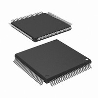
MCU 3/5V 0K I-TEMP 100-LQFP
Manufacturer
Renesas Electronics America
Series
M16C™ M32C/80r
Datasheet
1.M30800SAFPU5.pdf
(62 pages)
Specifications of M30800SAGP#D3
Core Processor
M16C/80
Core Size
16-Bit
Speed
20MHz
Connectivity
I²C, IEBus, SIO, UART/USART
Peripherals
DMA, WDT
Number Of I /o
45
Program Memory Type
ROMless
Ram Size
8K x 8
Voltage - Supply (vcc/vdd)
3 V ~ 5.5 V
Data Converters
A/D 10x10b, D/A 2x8b
Oscillator Type
Internal
Operating Temperature
-40°C ~ 85°C
Package / Case
100-LQFP
Lead Free Status / RoHS Status
Contains lead / RoHS non-compliant
Eeprom Size
-
Program Memory Size
-
Available stocks
Company
Part Number
Manufacturer
Quantity
Price

Part Number:
M30800SAGP#D3M30800SAGP#U5
Manufacturer:
Renesas Electronics America
Quantity:
135
Part Number:
M30800SAGP#D3M30800SAGP#U5
Manufacturer:
Renesas Electronics America
Quantity:
10 000


M
R
R
1.6 Pin Description
e
E
3
. v
J
2
Table 1.4 Pin Description
I: Input
NOTE:
0
Power supply
Analog power
supply input
Reset input
CNV
External data
bus width
select input
Bus control
pins
C
1
3
Signal name
8 /
1 .
B
1. In this manual, hereafter, V
0
0
0
SS
0
G
3
N
8
o r
o
0 -
. v
u
O: Output
1
p
0
1
, 1
0
2
0
______
_________ ________
__________
________
V
V
AV
AV
____________
RESET
CNV
BYTE
D
D
A
A
A
A
A
A
CS0 to CS3
________ ______
WRL/WR
WRH/BHE
_____
RD
ALE
__________
HOLD
HLDA
RDY
______
Pin name I/O type
0
CC1,
SS
0
23
0
7
8
15
0
8
5
/D
/D
/D
CC
SS
to D
to D
to A
/D
SS
0
7
8
page 9
15
V
to
to
22
______
7
15
CC2
I/O: Input and output
CC
I/O
I/O
I/O
I/O
O
O
O
O
O
O
I
I
I
I
I
I
I
f o
refers to V
5
6
voltage
V
V
V
V
V
V
V
V
V
V
V
V
V
V
V
V
Supply
CC1
CC1
CC1
CC1
CC2
CC2
CC2
CC2
CC2
CC2
CC2
CC2
CC2
CC2
CC2
CC2
-
CC1
unless otherwise noted.
Apply 3.0 to 5.5 V to both V
V
Supplies power for the A/D converter. Connect the AV
V
The microcomputer is in a reset state when "L" is applied to the
____________
RESET pin
Connect this pin to V
Switches the data bus in external memory space 3. The data
bus is 16 bits long when the this pin is held "L" and 8 bits long
when the this pin is held "H". Set it to either one.
Inputs and outputs data (D
memory space with separate bus
Inputs and outputs data (D
memory space with 16-bit separate bus
Outputs address bits (A
Outputs inversed address bit A23
Inputs and outputs data (D
address bits (A
external memory space with multiplexed bus
Inputs and outputs data (D
address bits (A
external memory space with multiplexed bus
Output CS0 to CS3 that are chip-select signals specifying an external space
Outputs WRL, WRH, (WR, BHE) and RD signals. WRL and WRH
can be switched with WR and BHE by program
If external data bus is 16 bits wide, data is writtenn to an even
address when WRL is held "L".
Data is written to an odd address when WRH is held "L".
Data is read when RD is held "L".
Data is written to external memory space when WR is held "L".
Data is read when RD is held "L".
An odd address is accessed when BHE is held "L".
Select WR, BHE and RD for an external 8-bit data bus
ALE is a signal latching address
The microcomputer is placed in a hold state while the HOLD pin
is held "L"
Outputs an "L" siganl while the microcomputer is placed in a hold state
Bus is placed in a wait state while the RDY pin is held "L"
SS
CC1
________
WRL, WRH and RD are selected:
______ ________
WR, BHE and RD are selected
pin. V
and the AV
______
______ ________
_________
_______
CC1
______
________
_______
0
8
V
to A
to A
SS
_____
CC2 (1)
_____
_____
_____
pin to V
7
15
CC1
______
_____
) by time-sharing while accessing an
______ ________
) by time-sharing while accessing an
0
to A
0
8
0
8
Description
CC1
SS
to D
to D
to D
to D
22)
_______
and V
7
15
7
15
) while accessing an external
) and outputs 8 low-order
) while accessing an external
) and outputs 8 middle-order
________
CC2
_____
________
pins. Apply 0 V to the
______
_______
__________
CC
1. Overview
pin to
________
Related parts for M30800SAGP#D3
Image
Part Number
Description
Manufacturer
Datasheet
Request
R

Part Number:
Description:
KIT STARTER FOR M16C/29
Manufacturer:
Renesas Electronics America
Datasheet:

Part Number:
Description:
KIT STARTER FOR R8C/2D
Manufacturer:
Renesas Electronics America
Datasheet:

Part Number:
Description:
R0K33062P STARTER KIT
Manufacturer:
Renesas Electronics America
Datasheet:

Part Number:
Description:
KIT STARTER FOR R8C/23 E8A
Manufacturer:
Renesas Electronics America
Datasheet:

Part Number:
Description:
KIT STARTER FOR R8C/25
Manufacturer:
Renesas Electronics America
Datasheet:

Part Number:
Description:
KIT STARTER H8S2456 SHARPE DSPLY
Manufacturer:
Renesas Electronics America
Datasheet:

Part Number:
Description:
KIT STARTER FOR R8C38C
Manufacturer:
Renesas Electronics America
Datasheet:

Part Number:
Description:
KIT STARTER FOR R8C35C
Manufacturer:
Renesas Electronics America
Datasheet:

Part Number:
Description:
KIT STARTER FOR R8CL3AC+LCD APPS
Manufacturer:
Renesas Electronics America
Datasheet:
Part Number:
Description:
KIT STARTER FOR RX610
Manufacturer:
Renesas Electronics America
Datasheet:

Part Number:
Description:
KIT STARTER FOR R32C/118
Manufacturer:
Renesas Electronics America
Datasheet:

Part Number:
Description:
KIT DEV RSK-R8C/26-29
Manufacturer:
Renesas Electronics America
Datasheet:

Part Number:
Description:
KIT STARTER FOR SH7124
Manufacturer:
Renesas Electronics America
Datasheet:

Part Number:
Description:
KIT STARTER FOR H8SX/1622
Manufacturer:
Renesas Electronics America
Datasheet:

Part Number:
Description:
KIT DEV FOR SH7203
Manufacturer:
Renesas Electronics America
Datasheet: