M30800SAGP#D3 Renesas Electronics America, M30800SAGP#D3 Datasheet - Page 53
M30800SAGP#D3
Manufacturer Part Number
M30800SAGP#D3
Description
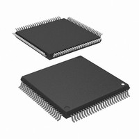
MCU 3/5V 0K I-TEMP 100-LQFP
Manufacturer
Renesas Electronics America
Series
M16C™ M32C/80r
Datasheet
1.M30800SAFPU5.pdf
(62 pages)
Specifications of M30800SAGP#D3
Core Processor
M16C/80
Core Size
16-Bit
Speed
20MHz
Connectivity
I²C, IEBus, SIO, UART/USART
Peripherals
DMA, WDT
Number Of I /o
45
Program Memory Type
ROMless
Ram Size
8K x 8
Voltage - Supply (vcc/vdd)
3 V ~ 5.5 V
Data Converters
A/D 10x10b, D/A 2x8b
Oscillator Type
Internal
Operating Temperature
-40°C ~ 85°C
Package / Case
100-LQFP
Lead Free Status / RoHS Status
Contains lead / RoHS non-compliant
Eeprom Size
-
Program Memory Size
-
Available stocks
Company
Part Number
Manufacturer
Quantity
Price

Part Number:
M30800SAGP#D3M30800SAGP#U5
Manufacturer:
Renesas Electronics America
Quantity:
135
Part Number:
M30800SAGP#D3M30800SAGP#U5
Manufacturer:
Renesas Electronics America
Quantity:
10 000


R
R
M
e
E
3
. v
J
2
Switching Characteristics
Table 5.38 Memory Expansion Mode and Microprocessor Mode
NOTES:
d t
h t
h t
h t
d t
h t
h t
h t
d t
h t
d t
h t
d t
h t
d t
h t
d t
h t
t
0
z d
C
1
3
B (
B (
R (
(
B (
B (
R (
(
B (
B (
B (
B (
D (
(
B (
B (
A (
A (
W
W
W
1 .
8 /
S
B
R (
(V
C
C
C
C
C
C
C
C
C
C
D
L
D
D
- B
R
R
R
1. Values can be obtained by the following equations, according to BLCK frequency.
y
2. Values can be obtained by the following equations, according to BLCK frequency and external bus cycles.
3. Values can be obtained by the following equations, according to BLCK frequency and external bus cycles.
E
4. Values can be obtained by the following equations, according to BLCK frequency and external bus cycles.
0
0
L
L
L
L
L
L
L
L
L
L
A -
A -
C -
D
0
A -
C -
D -
W
m
A -
K
K
K
K
K
K
- K
- K
K
K
0
CC1
A -
) D
L
) S
A -
A -
C -
C -
R -
R -
A -
A -
) D
) S
) R
) B
3
) D
G
W
W
) E
N
b
) D
) D
) D
) S
) S
) D
) D
L
L
8
l o
) R
) R
t
t
t
t
t
t
t
t
o
) E
) E
o r
h(RD – AD)
h(WR – AD)
h(RD – CS)
h(WR – CS)
h(WR – DB)
d(DB – WR)
d(AD – ALE)
h(ALE – AD)
0 -
. v
= V
u
1
0
1
p
R
R
D
D
A
A
A
A
C
C
C
C
W
W
A
A
A
A
A
, 1
0
CC2
d
d
d
d
D
D
a
a
L
L
L
L
d
h
h
h
h
(when accessing an external memory space with the multiplexed bus)
R
R
2
d
d
d
d
a t
a t
E
E
E
E
d
p i
p i
p i
p i
S
S
0
e r
e r
e r
e r
e r
S
S
S -
S -
S -
S -
=
=
S
S
S
S
=
=
=
=
g i
g i
O
O
0
=
= 3.0 to 3.6V, VSS = 0V at Topr = –20 to 85
=
s s
s s
s s
s s
g i
g i
s s
g i
g i
g i
g i
5
e
e
e
e
n
n
u
u
n
n
e l
e l
e l
e l
n
n
n
n
l a
l a
p t
p t
O
O
O
O
l a
l a
O
10 X m
f
f
l a
l a
l a
l a
f
f
f
f
f
t c
t c
t c
t c
(BCLK)
(BCLK)
Page 51
f
(BCLK)
(BCLK)
(BCLK)
(BCLK)
(BCLK)
t u
t u
(BCLK)
u
u
u
u
O
O
u
10 x n
O
O
10 x n
9
O
O
O
O
p t
p t
p t
p t
p t
S
S
S
S
u
u
d
H
9
u
u
10
10
10
10
10
u
u
u
u
t u
t u
t u
t u
g i
g i
g i
g i
p t
p t
t u
9
l e
p t
p t
o
p t
p t
p t
p t
n
n
n
n
t u
t u
y a
d l
X 2
X 2
t u
t u
9
9
9
9
D
H
H
H
F
9
X 2
X 2
X 2
X 2
X 2
l a
l a
l a
l a
t u
t u
t u
t u
X 2
o l
l e
o
o
o
T
D
H
D
H
T
d l
d l
d l
O
O
O
O
m i
D
H
D
H
t a
y a
l e
o
m i
l e
o
u
u
u
u
d l
l e
o
l e
o
f o
y a
T
T
T
d l
e
S
p t
p t
p t
p t
y a
d l
d l
– 25
– 10
– 10
–10
– 10
– 20
– 20
– 10
e
y a
y a
T
m i
m i
m i
T
a t
(
5
t u
t u
t u
t u
T
m i
P
(
W
T
T
T
m i
6
T
W
e
e
e
t r
m i
T
T
m i
m i
m i
a
e
m i
R
D
H
H
H
e
m i
m i
a r
R
B (
R (
(
T
e
W
l e
o
o
o
e
e
e
s
m i
e
m
[ns] (if external bus cycle is a + b , m=(b+2)-1)
[ns] (if external bus cycle is a + b , n=a)
d l
d l
d l
e
e
[ns]
[ns]
[ns]
[ns]
[ns]
[ns] (if external bus cycle is a + b , n=a)
C
s
D
y a
a t
R
B (
a (
a t
t e
L
e
B (
a (
n
s
T
T
T
d
K
s
C
n
r e
T
a t
d
m i
m i
m i
d
a t
C
d
d
L
r a
m i
s
d
e r
n
r a
L
K
n
e
e
e
a t
e r
d
) d
K
d
e
s s
) d
r a
B (
R (
(
s
n
s s
r a
W
s
a t
d
) d
s
C
a t
) d
D
r a
R
n
s
a t
L
n
d
a t
) d
s
K
n
s
d
r a
a t
a t
n
d
r a
s
) d
d
r a
n
n
a t
) d
r a
d
d
) d
r a
n
r a
) d
d
) d
) d
r a
) d
o
C unless otherwise specified)
See Figure 5.1
M
e
C
a
o
u s
n
i d
e r
o i t
m
n
e
t n
5. Electrical Characteristics
N (
N (
N (
N (
N (
N (
N (
N (
M
o
o
o
o
o
o
o
o
3 -
2 -
0
0
0
e t
e t
e t
e t
e t
e t
e t
e t
. n i
V
S
CC1
) 1
) 1
) 1
) 1
) 2
) 1
) 3
) 4
a t
n
d
a
=V
d r
M
1
1
1
1
1
8
a
8
8
8
8
8
CC2
. x
=3.3V
U
s n
s n
s n
s n
s n
s n
s n
s n
s n
s n
s n
s n
s n
s n
s n
s n
s n
s n
s n
t i n
Related parts for M30800SAGP#D3
Image
Part Number
Description
Manufacturer
Datasheet
Request
R

Part Number:
Description:
KIT STARTER FOR M16C/29
Manufacturer:
Renesas Electronics America
Datasheet:

Part Number:
Description:
KIT STARTER FOR R8C/2D
Manufacturer:
Renesas Electronics America
Datasheet:

Part Number:
Description:
R0K33062P STARTER KIT
Manufacturer:
Renesas Electronics America
Datasheet:

Part Number:
Description:
KIT STARTER FOR R8C/23 E8A
Manufacturer:
Renesas Electronics America
Datasheet:

Part Number:
Description:
KIT STARTER FOR R8C/25
Manufacturer:
Renesas Electronics America
Datasheet:

Part Number:
Description:
KIT STARTER H8S2456 SHARPE DSPLY
Manufacturer:
Renesas Electronics America
Datasheet:

Part Number:
Description:
KIT STARTER FOR R8C38C
Manufacturer:
Renesas Electronics America
Datasheet:

Part Number:
Description:
KIT STARTER FOR R8C35C
Manufacturer:
Renesas Electronics America
Datasheet:

Part Number:
Description:
KIT STARTER FOR R8CL3AC+LCD APPS
Manufacturer:
Renesas Electronics America
Datasheet:
Part Number:
Description:
KIT STARTER FOR RX610
Manufacturer:
Renesas Electronics America
Datasheet:

Part Number:
Description:
KIT STARTER FOR R32C/118
Manufacturer:
Renesas Electronics America
Datasheet:

Part Number:
Description:
KIT DEV RSK-R8C/26-29
Manufacturer:
Renesas Electronics America
Datasheet:

Part Number:
Description:
KIT STARTER FOR SH7124
Manufacturer:
Renesas Electronics America
Datasheet:

Part Number:
Description:
KIT STARTER FOR H8SX/1622
Manufacturer:
Renesas Electronics America
Datasheet:

Part Number:
Description:
KIT DEV FOR SH7203
Manufacturer:
Renesas Electronics America
Datasheet: