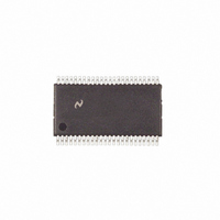
COP8CFE9IMT9/NOPB National Semiconductor, COP8CFE9IMT9/NOPB Datasheet - Page 36

COP8CFE9IMT9/NOPB
Manufacturer Part Number
COP8CFE9IMT9/NOPB
Description
IC MCU EEPROM 8BIT 8K 48-TSSOP
Manufacturer
National Semiconductor
Series
COP8™ 8Cr
Datasheet
1.COP8-EMFA-28N.pdf
(63 pages)
Specifications of COP8CFE9IMT9/NOPB
Core Processor
COP8
Core Size
8-Bit
Connectivity
Microwire/Plus (SPI)
Peripherals
POR, PWM, WDT
Number Of I /o
39
Program Memory Size
8KB (8K x 8)
Program Memory Type
FLASH
Ram Size
256 x 8
Voltage - Supply (vcc/vdd)
2.7 V ~ 5.5 V
Data Converters
A/D 16x10b
Oscillator Type
Internal
Operating Temperature
0°C ~ 70°C
Package / Case
48-TSSOP
Lead Free Status / RoHS Status
Lead free / RoHS Compliant
Speed
-
Eeprom Size
-
Other names
*COP8CFE9IMT9
*COP8CFE9IMT9/NOPB
COP8CFE9IMT9
*COP8CFE9IMT9/NOPB
COP8CFE9IMT9
www.national.com
8.0 A/D Converter
MODE SELECT
This 1-bit field is used to select the mode of operation (single
ended or differential) as shown in the following Table 20 .
PRESCALER SELECT
This 1-bit field is used to select one of two prescaler clocks
for the A/D Converter. The following Table 21 shows the
various prescaler options. Care must be taken, when select-
ing this bit, to keep the A/D clock frequency within the
specified range.
BUSY BIT
The ADBSY bit of the ENAD register is used to control
starting and stopping of the A/D conversion. When ADBSY is
cleared, the prescale logic is disabled and the A/D clock is
turned off, drawing minimal power. Setting the ADBSY bit
starts the A/D clock and initiates a conversion based on the
TABLE 20. A/D Conversion Mode Selection
TABLE 21. A/D Converter Clock Prescale
ADMOD
PSC
0
1
0
1
FIGURE 20. A/D with Single Ended Mux Output Feature Enabled
FIGURE 21. A/D with Differential Mux Output Feature Enabled
(Continued)
Single Ended Mode
MCLK Divide by 16
MCLK Divide by 1
Differential Mode
Clock Select
Mode
36
values currently in the ENAD register. Normal completion of
an A/D conversion clears the ADBSY bit and turns off the A/D
Converter.
If the user wishes to restart a conversion which is already in
progress, this can be accomplished only by writing a zero to
the ADBSY bit to stop the current conversion and then by
writing a one to ADBSY to start a new conversion. This can
be done in two consecutive instructions.
9.1.2 A/D Result Registers
There are two result registers for the A/D converter: the high
8 bits of the result and the low 2-bits of the result. The format
of these registers is shown in Figures 21, 22 . Both registers
are read/write registers, but in normal operation, the hard-
ware writes the value into the register when the conversion is
complete and the software reads the value. Both registers
are undefined upon Reset. They hold the previous value until
a new conversion overwrites them. When reading ADRSTL,
bits 5-0 will read as 0.
Bit 7
Bit 7
Bit 9
Bit 1
Bit 8
Bit 0
Bit 7
0
20026429
TABLE 22. ADRSTH
TABLE 23. ADRSTL
20026430
Bit 6
0
Bit 5
0
Bit 4
0
Bit 3
0
Bit 0
Bit 0
Bit 2
0


