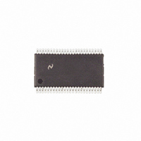
COP8CFE9IMT9/NOPB National Semiconductor, COP8CFE9IMT9/NOPB Datasheet - Page 11

COP8CFE9IMT9/NOPB
Manufacturer Part Number
COP8CFE9IMT9/NOPB
Description
IC MCU EEPROM 8BIT 8K 48-TSSOP
Manufacturer
National Semiconductor
Series
COP8™ 8Cr
Datasheet
1.COP8-EMFA-28N.pdf
(63 pages)
Specifications of COP8CFE9IMT9/NOPB
Core Processor
COP8
Core Size
8-Bit
Connectivity
Microwire/Plus (SPI)
Peripherals
POR, PWM, WDT
Number Of I /o
39
Program Memory Size
8KB (8K x 8)
Program Memory Type
FLASH
Ram Size
256 x 8
Voltage - Supply (vcc/vdd)
2.7 V ~ 5.5 V
Data Converters
A/D 16x10b
Oscillator Type
Internal
Operating Temperature
0°C ~ 70°C
Package / Case
48-TSSOP
Lead Free Status / RoHS Status
Lead free / RoHS Compliant
Speed
-
Eeprom Size
-
Other names
*COP8CFE9IMT9
*COP8CFE9IMT9/NOPB
COP8CFE9IMT9
*COP8CFE9IMT9/NOPB
COP8CFE9IMT9
MICROWIRE/PLUS Output Propagation Delay
(t
Input Pulse Width
Output Pulse Width
Reset Pulse Width
t
Note 10: Maximum rate of voltage change must be
Note 11: Supply and IDLE currents are measured with CKI driven with a square wave Oscillator, CKO driven 180˚ out of phase with CKI, inputs connected to V
and outputs driven low but not connected to a load.
Note 12: The HALT mode will stop CKI from oscillating. Measurement of I
G0, and G2–G5 programmed as low outputs and not driving a load; all D outputs programmed low and not driving a load; all inputs tied to V
clock monitor and BOR disabled. Parameter refers to HALT mode entered via setting bit 7 of the G Port data register.
Note 13: Pins G6 and RESET are designed with a high voltage input network. These pins allow input voltages
when biased at voltages
must be limited to
Note 14: If timer is in high speed mode, the minimum time is 1 MCLK. If timer is not in high speed mode, the minimum time is 1 t
Note 15: Absolute Maximum Ratings should not be exceeded.
Note 16: V
UPD
Datasheet min/max specification limits are guaranteed by design, test, or statistical analysis.
C
Interrupt Input High Time
Interrupt Input Low Time
Timer 1 Input High Time
Timer 1 Input Low Time
Timer 2, 3 Input High Time (Note 6)
Timer 2, 3 Input Low Time (Note 6)
Timer 2, 3 Output High Time
Timer 2, 3 Output Low Time
= instruction cycle time.
)
cc
must be valid and stable before G6 is raised to a high voltage.
<
(V
Parameter
CC
>
+ 7V. WARNING: Voltages in excess of 14V will cause damage to the pins. This warning excludes ESD transients.
V
CC
(the pins do not have source current when biased at a voltage below V
AC Electrical Characteristics (−40˚C
<
0.5 V/ms.
Conditions
DD
HALT is done with device neither sourcing nor sinking current; with L. A. B, C, E, F,
11
T
A
+125˚C) (Continued)
CC
). These two pins will not latch up. The voltage at the pins
Min
150
150
0.5
1
1
1
1
1
1
>
V
CC
Typ
and the pins will have sink current to V
C
Max
150
.
CC
; A/D converter and
MCLK or t
MCLK or t
www.national.com
Units
ns
ns
ns
t
t
t
t
t
C
C
C
C
C
C
C
CC
CC


