ST7FMC1K2TCE STMicroelectronics, ST7FMC1K2TCE Datasheet - Page 219
ST7FMC1K2TCE
Manufacturer Part Number
ST7FMC1K2TCE
Description
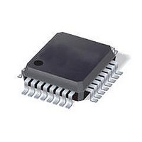
IC MCU 8BIT 8K FLASH 32-LQFP
Manufacturer
STMicroelectronics
Series
ST7r
Datasheet
1.ST7FMC2S4T6.pdf
(309 pages)
Specifications of ST7FMC1K2TCE
Core Processor
ST7
Core Size
8-Bit
Speed
8MHz
Connectivity
LINSCI
Peripherals
LVD, Motor Control PWM, POR, PWM, WDT
Number Of I /o
17
Program Memory Size
8KB (8K x 8)
Program Memory Type
FLASH
Ram Size
384 x 8
Voltage - Supply (vcc/vdd)
3.8 V ~ 5.5 V
Data Converters
A/D 16x10b
Oscillator Type
External
Operating Temperature
-40°C ~ 125°C
Package / Case
32-LQFP
For Use With
497-8402 - BOARD EVAL COMPLETE INVERTER497-8400 - KIT IGBT PWR MODULE CTRL ST7MC497-4734 - EVAL KIT 3KW POWER DRIVER BOARD497-4733 - EVAL KIT 1KW POWER DRIVER BOARD497-4732 - EVAL KIT 300W POWER DRIVER BOARD497-4731 - EVAL KIT PWR DRIVER CONTROL BRD
Lead Free Status / RoHS Status
Lead free / RoHS Compliant
Eeprom Size
-
Lead Free Status / Rohs Status
Lead free / RoHS Compliant
Available stocks
Company
Part Number
Manufacturer
Quantity
Price
Company:

Part Number:
ST7FMC1K2TCE
Manufacturer:
STMicroelectronics
Quantity:
10 000


MOTOR CONTROLLER (Cont’d)
REPETITION COUNTER REGISTER (MREP)
Read/Write
Reset Value: 0000 0000 (00h)
Bits 7:0 = REP[7:0] Repetition counter value (N).
This register allows the user to set-up the update
rate of the PWM counter compare register (i.e. pe-
riodic transfers from preload to active registers),
as well as the PWM Update interrupt generation
rate, if these interrupts are enabled.
Each time the MREP related Down-Counter
reaches zero, the Compare registers are updated,
a U interrupt is generated and it re-starts counting
from the MREP value.
After a microcontroller reset, setting the CKE bit in
the MCRA register (i.e. enabling the clock for the
MTC peripheral) forces the transfer from the
MREP preload register to its active register and
generates a U interrupt. During run-time (while
CKE bit = 1) a new value entered in the MREP
preload register is taken into account after a U
event.
As shown in
to:
– The number of PWM periods in edge-aligned
– The number of half PWM periods in center-
–
COMPARE PHASE W PRELOAD REGISTER
HIGH (MCPWH)
Read/Write
Reset Value: 0000 0000 (00h)
Bits 7:0 = CPWH[7:0] Most Significant Byte of
phase W preload value
CPWH
REP7 REP6 REP5 REP4
mode
aligned mode.
7
7
7
CPWH
6
Figure
CPWH
5
CPWH
122, (N+1) value corresponds
4
REP3
CPWH
3
REP2
CPWH
2
REP1
CPWH
1
CPWH
REP0
0
0
0
COMPARE PHASE W PRELOAD REGISTER
LOW (MCPWL)
Read/Write (except bits 2:0)
Reset Value: 0000 0000 (00h)
Bits 7:5 = CPWL[7:3] Low bits of phase W preload
value.
Bits 2:0 = Reserved.
COMPARE PHASE V PRELOAD REGISTER
HIGH (MCPVH)
Read/Write
Reset Value: 0000 0000 (00h)
Bit 7:0 = CPVH[7:0] Most Significant Byte of
phase V preload value
COMPARE PHASE V PRELOAD REGISTER
LOW (MCPVL)
Read/Write (except bits 2:0)
Reset Value: 0000 0000 (00h)
Bits 7:5 = CPVL[7:3] Low bits of phase V preload
value.
Bits 2:0 = Reserved.
CPVH7 CPVH6 CPVH5 CPVH4 CPVH3 CPVH2 CPVH1 CPVH0
CPVL7 CPVL6 CPVL5 CPVL4 CPVL3
CPWL
7
7
7
7
CPWL
6
CPWL
5
CPWL
4
ST7MC1xx/ST7MC2xx
CPWL
3
-
-
-
-
219/309
0
0
0
-
-
Related parts for ST7FMC1K2TCE
Image
Part Number
Description
Manufacturer
Datasheet
Request
R

Part Number:
Description:
STMicroelectronics [RIPPLE-CARRY BINARY COUNTER/DIVIDERS]
Manufacturer:
STMicroelectronics
Datasheet:
Part Number:
Description:
STMicroelectronics [LIQUID-CRYSTAL DISPLAY DRIVERS]
Manufacturer:
STMicroelectronics
Datasheet:

Part Number:
Description:
BOARD EVAL FOR MEMS SENSORS
Manufacturer:
STMicroelectronics
Datasheet:
Part Number:
Description:
NPN TRANSISTOR POWER MODULE
Manufacturer:
STMicroelectronics
Datasheet:
Part Number:
Description:
TURBOSWITCH ULTRA-FAST HIGH VOLTAGE DIODE
Manufacturer:
STMicroelectronics
Datasheet:
Part Number:
Description:
Manufacturer:
STMicroelectronics
Datasheet:
Part Number:
Description:
DIODE / SCR MODULE
Manufacturer:
STMicroelectronics
Datasheet:
Part Number:
Description:
DIODE / SCR MODULE
Manufacturer:
STMicroelectronics
Datasheet:
Part Number:
Description:
Search -----> STE16N100
Manufacturer:
STMicroelectronics
Datasheet:
Part Number:
Description:
Search ---> STE53NA50
Manufacturer:
STMicroelectronics
Datasheet:
Part Number:
Description:
NPN Transistor Power Module
Manufacturer:
STMicroelectronics
Datasheet:
Part Number:
Description:
DIODE / SCR MODULE
Manufacturer:
STMicroelectronics
Datasheet: