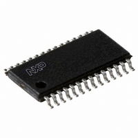
P89LPC936FDH,529 NXP Semiconductors, P89LPC936FDH,529 Datasheet - Page 10

P89LPC936FDH,529
Manufacturer Part Number
P89LPC936FDH,529
Description
IC 80C51 MCU FLASH 16K 28-TSSOP
Manufacturer
NXP Semiconductors
Series
LPC900r
Datasheet
1.P89LPC936FDH518.pdf
(77 pages)
Specifications of P89LPC936FDH,529
Core Processor
8051
Core Size
8-Bit
Speed
18MHz
Connectivity
I²C, SPI, UART/USART
Peripherals
Brown-out Detect/Reset, LED, POR, PWM, WDT
Number Of I /o
26
Program Memory Size
16KB (16K x 8)
Program Memory Type
FLASH
Eeprom Size
512 x 8
Ram Size
768 x 8
Voltage - Supply (vcc/vdd)
2.4 V ~ 3.6 V
Data Converters
A/D 8x8b; D/A 2x8b
Oscillator Type
Internal
Operating Temperature
-40°C ~ 85°C
Package / Case
28-TSSOP
For Use With
622-1014 - BOARD FOR LPC9XX TSSOP622-1008 - BOARD FOR LPC9103 10-HVSON622-1006 - SOCKET ADAPTER BOARDMCB900K - BOARD PROTOTYPE NXP 89LPC9EPM900K - EMULATOR/PROGRAMMER NXP P89LPC9568-1759 - EMULATOR DEBUGGER/PROGRMMR LPC9X568-1758 - BOARD EVAL FOR LPC93X MCU FAMILY
Lead Free Status / RoHS Status
Lead free / RoHS Compliant
Other names
568-2012-5
935277841529
P89LPC936FDH-S
935277841529
P89LPC936FDH-S
NXP Semiconductors
Table 4.
[1]
P89LPC933_934_935_936
Product data sheet
Symbol
P3.0 to P3.1
P3.0/XTAL2/
CLKOUT
P3.1/XTAL1
V
V
SS
DD
Input/output for P1.0 to P1.4, P1.6, P1.7. Input for P1.5.
Pin description
Pin
TSSOP28,
PLCC28
9
8
7
21
4
HVQFN28
5
3
17
…continued
Type
I/O
O
O
I/O
I
I
I
I/O
All information provided in this document is subject to legal disclaimers.
Description
Port 3: Port 3 is a 2-bit I/O port with a user-configurable output type.
During reset Port 3 latches are configured in the input only mode with the
internal pull-up disabled. The operation of Port 3 pins as inputs and
outputs depends upon the port configuration selected. Each port pin is
configured independently. Refer to
and
All pins have Schmitt trigger inputs.
Port 3 also provides various special functions as described below:
P3.0 — Port 3 bit 0.
XTAL2 — Output from the oscillator amplifier (when a crystal oscillator
option is selected via the flash configuration.
CLKOUT — CPU clock divided by 2 when enabled via SFR bit (ENCLK -
TRIM.6). It can be used if the CPU clock is the internal RC oscillator,
watchdog oscillator or external clock input, except when XTAL1/XTAL2
are used to generate clock source for the RTC/system timer.
P3.1 — Port 3 bit 1.
XTAL1 — Input to the oscillator circuit and internal clock generator circuits
(when selected via the flash configuration). It can be a port pin if internal
RC oscillator or watchdog oscillator is used as the CPU clock source, and
if XTAL1/XTAL2 are not used to generate the clock for the RTC/system
timer.
Ground: 0 V reference.
Power supply: This is the power supply voltage for normal operation as
well as Idle and Power-down modes.
Rev. 8 — 12 January 2011
8-bit microcontroller with accelerated two-clock 80C51 core
Table 11 “Static characteristics”
P89LPC933/934/935/936
Section 8.13.1 “Port configurations”
for details.
© NXP B.V. 2011. All rights reserved.
10 of 77


