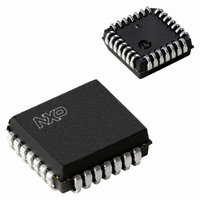
P89LPC932A1FA,129 NXP Semiconductors, P89LPC932A1FA,129 Datasheet - Page 8

P89LPC932A1FA,129
Manufacturer Part Number
P89LPC932A1FA,129
Description
IC 80C51 MCU FLASH 8K 28-PLCC
Manufacturer
NXP Semiconductors
Series
LPC900r
Datasheet
1.P89LPC932A1FDH529.pdf
(64 pages)
Specifications of P89LPC932A1FA,129
Core Processor
8051
Core Size
8-Bit
Speed
18MHz
Connectivity
I²C, SPI, UART/USART
Peripherals
Brown-out Detect/Reset, LED, POR, PWM, WDT
Number Of I /o
26
Program Memory Size
8KB (8K x 8)
Program Memory Type
FLASH
Ram Size
768 x 8
Voltage - Supply (vcc/vdd)
2.4 V ~ 3.6 V
Oscillator Type
Internal
Operating Temperature
-40°C ~ 85°C
Package / Case
28-PLCC
For Use With
OM6292 - DEMO BOARD PCA2125 RTCDB-TSSOP-LPC932 - BOARD FOR LPC932 TSSOP622-1014 - BOARD FOR LPC9XX TSSOP622-1008 - BOARD FOR LPC9103 10-HVSON622-1006 - SOCKET ADAPTER BOARDMCB900K - BOARD PROTOTYPE NXP 89LPC9EPM900K - EMULATOR/PROGRAMMER NXP P89LPC9622-1003 - KIT FOR LCD DEMO568-1759 - EMULATOR DEBUGGER/PROGRMMR LPC9X568-1758 - BOARD EVAL FOR LPC93X MCU FAMILY
Lead Free Status / RoHS Status
Lead free / RoHS Compliant
Eeprom Size
-
Data Converters
-
Other names
568-1285-5
935276131129
P89LPC932A1FA-S
935276131129
P89LPC932A1FA-S
Available stocks
Company
Part Number
Manufacturer
Quantity
Price
Company:
Part Number:
P89LPC932A1FA,129
Manufacturer:
NXP Semiconductors
Quantity:
10 000
NXP Semiconductors
Table 2.
P89LPC932A1_3
Product data sheet
Symbol
P0.4/ CIN1A/
KBI4
P0.5/
CMPREF/
KBI5
P0.6/CMP1/
KBI6
P0.7/T1/KBI7
P1.0 to P1.7
P1.0/TXD
P1.1/RXD
P1.2/T0/SCL
P1.3/INT0/
SDA
P1.4/INT1
Pin description
Pin
TSSOP28,
PLCC28,
DIP28
23
22
20
19
18
17
12
11
10
…continued
HVQFN28
19
18
16
15
14
13
8
7
6
Type Description
I/O
I
I
I/O
I
I
I/O
O
I
I/O
I/O
I
I/O, I
[1]
I/O
O
I/O
I
I/O
I/O
I/O
I/O
I
I/O
I
I
P0.4 — Port 0 bit 4.
CIN1A — Comparator 1 positive input A.
KBI4 — Keyboard input 4.
P0.5 — Port 0 bit 5.
CMPREF — Comparator reference (negative) input.
KBI5 — Keyboard input 5.
P0.6 — Port 0 bit 6.
CMP1 — Comparator 1 output.
KBI6 — Keyboard input 6.
P0.7 — Port 0 bit 7.
T1 — Timer/counter 1 external count input or overflow output.
KBI7 — Keyboard input 7.
Port 1: Port 1 is an 8-bit I/O port with a user-configurable output type,
except for three pins as noted below. During reset Port 1 latches are
configured in the input only mode with the internal pull-up disabled. The
operation of the configurable Port 1 pins as inputs and outputs depends
upon the port configuration selected. Each of the configurable port pins
are programmed independently. Refer to
configurations”
P1.3 are open drain when used as outputs. P1.5 is input only.
All pins have Schmitt trigger inputs.
Port 1 also provides various special functions as described below:
P1.0 — Port 1 bit 0.
TXD — Transmitter output for the serial port.
P1.1 — Port 1 bit 1.
RXD — Receiver input for the serial port.
P1.2 — Port 1 bit 2 (open-drain when used as output).
T0 — Timer/counter 0 external count input or overflow output (open-drain
when used as output).
SCL — I
P1.3 — Port 1 bit 3 (open-drain when used as output).
INT0 — External interrupt 0 input.
SDA — I
P1.4 — Port 1 bit 4.
INT1 — External interrupt 1 input.
Rev. 03 — 12 March 2007
8-bit microcontroller with accelerated two-clock 80C51 core
2
2
C serial clock input/output.
C serial data input/output.
and
Table 8 “Static characteristics”
Section 7.13.1 “Port
P89LPC932A1
for details. P1.2 and
© NXP B.V. 2007. All rights reserved.
8 of 64


