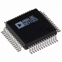
ADUC831BS Analog Devices Inc, ADUC831BS Datasheet - Page 66

ADUC831BS
Manufacturer Part Number
ADUC831BS
Description
IC ADC/DAC 12BIT W/MCU 52-MQFP
Manufacturer
Analog Devices Inc
Series
MicroConverter® ADuC8xxr
Datasheet
1.EVAL-ADUC831QSZ.pdf
(76 pages)
Specifications of ADUC831BS
Rohs Status
RoHS non-compliant
Core Processor
8052
Core Size
8-Bit
Speed
16MHz
Connectivity
EBI/EMI, I²C, SPI, UART/USART
Peripherals
PSM, Temp Sensor, WDT
Number Of I /o
34
Program Memory Size
62KB (62K x 8)
Program Memory Type
FLASH
Eeprom Size
4K x 8
Ram Size
2.25K x 8
Voltage - Supply (vcc/vdd)
2.7 V ~ 5.5 V
Data Converters
A/D 8x12b, D/A 2x12b
Oscillator Type
Internal
Operating Temperature
-40°C ~ 125°C
Package / Case
52-MQFP, 52-PQFP
For Use With
EVAL-ADUC831QSZ - KIT DEV FOR ADUC831 QUICK START
Available stocks
Company
Part Number
Manufacturer
Quantity
Price
Company:
Part Number:
ADUC831BS
Manufacturer:
SHARP
Quantity:
21 512
Company:
Part Number:
ADUC831BS
Manufacturer:
ADI
Quantity:
150
Part Number:
ADUC831BS
Manufacturer:
ADI/亚德诺
Quantity:
20 000
Company:
Part Number:
ADUC831BSB20
Manufacturer:
MINI
Quantity:
892
Company:
Part Number:
ADUC831BSZ
Manufacturer:
Analog Devices Inc
Quantity:
10 000
Part Number:
ADUC831BSZ
Manufacturer:
AD
Quantity:
20 000
Company:
Part Number:
ADUC831BSZ-REEL
Manufacturer:
AD
Quantity:
1 200
Company:
Part Number:
ADUC831BSZ-REEL
Manufacturer:
Analog Devices Inc
Quantity:
10 000
ADuC831
TIMING SPECIFICATIONS
Parameter
CLOCK INPUT (External Clock Driven XTAL1)
t
t
t
t
t
t
NOTES
1
2
3
4
AC inputs during testing are driven at DV
For timing purposes, a port pin is no longer floating when a 100 mV change from load voltage occurs. A port pin begins to float when a 100 mV change from the
C
ADuC831 Machine Cycle Time is nominally defined as MCLKIN/12.
CK
CKL
CKH
CKR
CKF
CYC
a Logic 0.
loaded V
LOAD
4
for Port0, ALE, PSEN outputs = 100 pF; C
OH
/V
OL
level occurs.
XTAL1 Period
XTAL1 Width Low
XTAL1 Width High
XTAL1 Rise Time
XTAL1 Fall Time
ADuC831 Machine Cycle Time
DV
DD
– 0.5V
0.45V
DD
– 0.5 V for a Logic 1 and 0.45 V for a Logic 0. Timing measurements are made at V
1, 2, 3
0.2DV
0.2DV
TEST POINTS
LOAD
Figure 69. Timing Waveform Characteristics
DD
DD
(AV
for all other outputs = 80 pF unless otherwise noted.
– 0.1V
+ 0.9V
t
CKH
DD
= DV
Figure 68. XTAL 1 Input
DD
= 3.0 V or 5.0 V
20
Min
20
–66–
t
V
CKL
12 MHz
LOAD
Typ
83.33
1
V
V
LOAD
LOAD
10%. All specifications T
t
– 0.1V
+ 0.1V
CKR
Max
20
20
t
CK
REFERENCE
Min
62.5
20
20
POINTS
TIMING
Variable Clock
t
CKF
A
Typ
12t
= T
CK
MIN
V
V
LOAD
LOAD
to T
IH
min for a Logic 1 and V
Max
1000
20
20
MAX
– 0.1V
– 0.1V
, unless otherwise noted.)
V
LOAD
Unit
ns
ns
ns
ns
ns
µs
IL
Figure
REV. 0
68
68
68
68
68
max for


