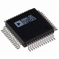
ADUC831BS Analog Devices Inc, ADUC831BS Datasheet - Page 34

ADUC831BS
Manufacturer Part Number
ADUC831BS
Description
IC ADC/DAC 12BIT W/MCU 52-MQFP
Manufacturer
Analog Devices Inc
Series
MicroConverter® ADuC8xxr
Datasheet
1.EVAL-ADUC831QSZ.pdf
(76 pages)
Specifications of ADUC831BS
Rohs Status
RoHS non-compliant
Core Processor
8052
Core Size
8-Bit
Speed
16MHz
Connectivity
EBI/EMI, I²C, SPI, UART/USART
Peripherals
PSM, Temp Sensor, WDT
Number Of I /o
34
Program Memory Size
62KB (62K x 8)
Program Memory Type
FLASH
Eeprom Size
4K x 8
Ram Size
2.25K x 8
Voltage - Supply (vcc/vdd)
2.7 V ~ 5.5 V
Data Converters
A/D 8x12b, D/A 2x12b
Oscillator Type
Internal
Operating Temperature
-40°C ~ 125°C
Package / Case
52-MQFP, 52-PQFP
For Use With
EVAL-ADUC831QSZ - KIT DEV FOR ADUC831 QUICK START
Available stocks
Company
Part Number
Manufacturer
Quantity
Price
Company:
Part Number:
ADUC831BS
Manufacturer:
SHARP
Quantity:
21 512
Company:
Part Number:
ADUC831BS
Manufacturer:
ADI
Quantity:
150
Part Number:
ADUC831BS
Manufacturer:
ADI/亚德诺
Quantity:
20 000
Company:
Part Number:
ADUC831BSB20
Manufacturer:
MINI
Quantity:
892
Company:
Part Number:
ADUC831BSZ
Manufacturer:
Analog Devices Inc
Quantity:
10 000
Part Number:
ADUC831BSZ
Manufacturer:
AD
Quantity:
20 000
Company:
Part Number:
ADUC831BSZ-REEL
Manufacturer:
AD
Quantity:
1 200
Company:
Part Number:
ADUC831BSZ-REEL
Manufacturer:
Analog Devices Inc
Quantity:
10 000
ADuC831
To reduce the effects of the saturation of the output amplifier at
values close to ground and to give reduced offset and gain errors,
the internal buffer can be bypassed. This is done by setting the
DBUF bit in the CFG831 register. This allows a full rail-to-rail
output from the DAC which should then be buffered externally
using a dual supply op-amp in order to get a rail-to-rail output.
This external buffer should be located as near as physically
possible to the DAC output pin on the PCB. Note the unbuffed
mode only works in the 0 to V
Figure 24. Source and Sink Current Capability with
V
REF
= V
3
2
1
0
0
DD
DAC LOADED WITH 0FFFH
DAC LOADED WITH 0000H
= 3 V
SOURCE/SINK CURRENT – mA
5
REF
range.
10
15
–34–
To drive significant loads with the DAC outputs, external buff-
ering may be required (even with the internal buffer enabled),
as illustrated in Figure 25. A list of recommended op-amps is in
Table VI.
The DAC output buffer also features a high-impedance disable
function. In the chip’s default power-on state, both DACs are
disabled, and their outputs are in a high-impedance state (or
“three-state”) where they remain inactive until enabled in software.
This means that if a zero output is desired during power-up or
power-down transient conditions, then a pull-down resistor must
be added to each DAC output. Assuming this resistor is in place,
the DAC outputs will remain at ground potential whenever the
DAC is disabled.
Figure 25. Buffering the DAC Outputs
DAC0
DAC1
ADuC831
REV. 0


