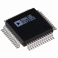
ADUC831BS Analog Devices Inc, ADUC831BS Datasheet - Page 3

ADUC831BS
Manufacturer Part Number
ADUC831BS
Description
IC ADC/DAC 12BIT W/MCU 52-MQFP
Manufacturer
Analog Devices Inc
Series
MicroConverter® ADuC8xxr
Datasheet
1.EVAL-ADUC831QSZ.pdf
(76 pages)
Specifications of ADUC831BS
Rohs Status
RoHS non-compliant
Core Processor
8052
Core Size
8-Bit
Speed
16MHz
Connectivity
EBI/EMI, I²C, SPI, UART/USART
Peripherals
PSM, Temp Sensor, WDT
Number Of I /o
34
Program Memory Size
62KB (62K x 8)
Program Memory Type
FLASH
Eeprom Size
4K x 8
Ram Size
2.25K x 8
Voltage - Supply (vcc/vdd)
2.7 V ~ 5.5 V
Data Converters
A/D 8x12b, D/A 2x12b
Oscillator Type
Internal
Operating Temperature
-40°C ~ 125°C
Package / Case
52-MQFP, 52-PQFP
For Use With
EVAL-ADUC831QSZ - KIT DEV FOR ADUC831 QUICK START
Available stocks
Company
Part Number
Manufacturer
Quantity
Price
Company:
Part Number:
ADUC831BS
Manufacturer:
SHARP
Quantity:
21 512
Company:
Part Number:
ADUC831BS
Manufacturer:
ADI
Quantity:
150
Part Number:
ADUC831BS
Manufacturer:
ADI/亚德诺
Quantity:
20 000
Company:
Part Number:
ADUC831BSB20
Manufacturer:
MINI
Quantity:
892
Company:
Part Number:
ADUC831BSZ
Manufacturer:
Analog Devices Inc
Quantity:
10 000
Part Number:
ADUC831BSZ
Manufacturer:
AD
Quantity:
20 000
Company:
Part Number:
ADUC831BSZ-REEL
Manufacturer:
AD
Quantity:
1 200
Company:
Part Number:
ADUC831BSZ-REEL
Manufacturer:
Analog Devices Inc
Quantity:
10 000
SPECIFICATIONS
Parameter
ADC CHANNEL SPECIFICATIONS
DC ACCURACY
CALIBRATED ENDPOINT ERRORS
DYNAMIC PERFORMANCE
ANALOG INPUT
TEMPERATURE SENSOR
DAC CHANNEL SPECIFICATIONS
DC ACCURACY
ANALOG OUTPUTS
DAC AC CHARACTERISTICS
REV. 0
Resolution
Integral Nonlinearity
Differential Nonlinearity
Integral Nonlinearity
Differential Nonlinearity
Code Distribution
Offset Error
Offset Error Match
Gain Error
Gain Error Match
Signal-to-Noise Ratio (SNR)
Total Harmonic Distortion (THD)
Peak Harmonic or Spurious Noise
Channel-to-Channel Crosstalk
Input Voltage Ranges
Leakage Current
Input Capacitance
Voltage Output at 25°C
Voltage TC
Accuracy
Internal Buffer Enabled
Resolution
Relative Accuracy
Differential Nonlinearity
Offset Error
Gain Error
Gain Error Mismatch
Voltage Range_0
Voltage Range_1
Output Impedance
Voltage Output Settling Time
Digital-to-Analog Glitch Energy
2, 3
10
4
4
11
9
7
8
1
(AV
all specifications T
DD
5, 6
= DV
V
12
± 1
± 0.3
± 0.9
± 0.25
± 1.5
+1.5/-0.9
1
± 4
± 1
± 2
–85
71
–85
–85
–80
0 to V
± 1
32
650
–2.0
± 3
± 1.5
12
± 3
–1
± 1/2
± 50
± 1
± 1
0.5
0 to V
0 to V
0.5
15
10
DD
DD
= 2.7 V to 3.3 V or 4.5 V to 5.5 V. V
= 5 V
REF
REF
DD
A
= T
MIN
to T
V
12
± 1
± 0.3
± 0.9
± 0.25
± 1.5
+1.5/–0.9
1
± 4
± 1
± 3
–85
71
–85
–85
–80
0 to V
± 1
32
650
–2.0
± 3
± 1.5
12
± 3
–1
± 1/2
± 50
± 1
± 1
0.5
0 to V
0 to V
0.5
15
10
DD
–3–
MAX
= 3 V
, unless otherwise noted.)
REF
REF
DD
Unit
LSB max
% typ
Bits
LSB max
LSB typ
LSB max
LSB typ
LSB max
LSB typ
LSB max
LSB typ
LSB max
dB typ
dB typ
dB typ
dB typ
dB typ
V
µA max
pF typ
mV typ
mV/°C typ
°C typ
°C typ
Bits
LSB typ
LSB max
LSB typ
mV max
% max
% typ
V typ
V typ
Ω typ
µs typ
nV sec typ
REF
= 2.5 V Internal Reference, MCLKIN = 16 MHz,
Test Conditions/Comments
f
Typical Performance at other f
2.5 V Internal Reference
2.5 V Internal Reference
1 V External Reference
1 V External Reference
ADC Input is a DC Voltage
f
f
Internal 2.5 V V
External 2.5 V V
DAC Load to AGND
R
Guaranteed 12-bit Monotonic
V
AV
V
% of Full Scale on DAC1
DAC V
DAC V
Full-Scale Settling Time to
within 1/2 LSB of Final Value
1 LSB Change at Major Carry
SAMPLE
IN
SAMPLE
L
REF
REF
= 10 kHz Sine Wave
= 10 kΩ, C
DD
Range
Range
Range
REF
REF
= 147 kHz, see Page 11 for
= 147 kHz
= 2.5 V
= V
L
DD
REF
= 100 pF
REF
ADuC831
SAMPLE


