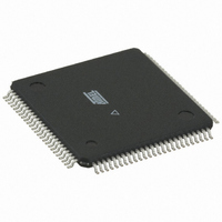
AT91R40807-33AU Atmel, AT91R40807-33AU Datasheet - Page 8

AT91R40807-33AU
Manufacturer Part Number
AT91R40807-33AU
Description
IC ARM7 MCU 100TQFP
Manufacturer
Atmel
Series
AT91SAMr
Datasheets
1.AT49LV1024-70VC.pdf
(15 pages)
2.AT91R40807-33AC.pdf
(19 pages)
3.AT91R40807-33AC.pdf
(20 pages)
Specifications of AT91R40807-33AU
Core Processor
ARM7
Core Size
16/32-Bit
Speed
33MHz
Connectivity
EBI/EMI, UART/USART
Peripherals
WDT
Number Of I /o
32
Program Memory Type
ROMless
Ram Size
136K x 8
Voltage - Supply (vcc/vdd)
1.8 V ~ 3.6 V
Oscillator Type
External
Operating Temperature
-40°C ~ 85°C
Package / Case
100-TQFP, 100-VQFP
Lead Free Status / RoHS Status
Lead free / RoHS Compliant
Eeprom Size
-
Program Memory Size
-
Data Converters
-
Available stocks
Company
Part Number
Manufacturer
Quantity
Price
Company:
Part Number:
AT91R40807-33AU
Manufacturer:
ATMEL
Quantity:
2 100
Product Overview
Power Supply
Input/Output
Considerations
Master Clock
Reset
NRST Pin
Watchdog Reset
Emulation Functions
Tri-state Mode
8
AT91R40807
The AT91R40807 microcontroller has a unique type of power supply pin
VDD pin supplies the I/O pads and the device core. The supported voltage range on V
is 1.8V to 3.6V.
The AT91R40807 accepts voltage levels up to the power supply limit on the pads.
After the reset, the peripheral I/Os are initialized as inputs to provide the user with maxi-
mum flexibility. It is recommended that in any application phase the inputs to the
AT91R40807 microcontroller be held at valid logic levels to minimize the power
consumption.
The AT91R40807 microcontroller has a fully static design and work on the Master Clock
(MCK), provided on the MCKI pin from an external source.
The Master Clock is also provided as an output of the device on the pin MCKO, which is
multiplexed with a general-purpose I/O line. While NRST is active, MCKO remains low.
After the reset, the MCKO is valid and outputs an image of the MCK signal. The PIO
controller must be programmed to use this pin as standard I/O line.
Reset restores the default states of the user interface registers (defined in the user inter-
face of each peripheral), and forces the ARM7TDMI to perform the next instruction fetch
from address zero. Except for the program counter the ARM7TDMI registers do not
have defined reset states.
NRST is active low-level input. It is asserted asynchronously, but exit from reset is syn-
chronized internally to the MCK. The signal presented on MCKI must be active within
the specification for a minimum of 10 clock cycles up to the rising edge of NRST to
ensure correct operation.
The first processor fetch occurs 80 clock cycles after the rising edge of NRST.
The watchdog can be programmed to generate an internal reset. In this case, the reset
has the same effect as the NRST pin assertion, but the pins BMS and NTRI are not
sampled. Boot mode and Tri-state mode are not updated. If the NRST pin is asserted
and the Watchdog triggers the internal reset, the NRST pin has priority.
The AT91R40807 provides a Tri-state mode, which is used for debug purposes. This
enables the connection of an emulator probe to an application board without having to
desolder the device from the target board. In Tri-state mode, all the output pin drivers of
the AT91R40807 microcontroller are disabled.
To enter Tri-state mode, the pin NTRI must be held low during the last 10 clock cycles
before the rising edge of NRST. For normal operation the pin NTRI must be held high
during reset, by a resistor of up to 400K Ohm.
NTRI is multiplexed with I/O line P21 and USART 1 serial data transmit line TXD1.
Standard RS232 drivers generally contain internal 400K Ohm pull-up resistors. If TXD1
is connected to a device not including this pull-up, the user must make sure that a high-
level is tied on NTRI while NRST is asserted.
1345DS–ATARM–02/02
–
VDD. The
DD


