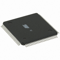
AT91R40807-33AU Atmel, AT91R40807-33AU Datasheet - Page 10

AT91R40807-33AU
Manufacturer Part Number
AT91R40807-33AU
Description
IC ARM7 MCU 100TQFP
Manufacturer
Atmel
Series
AT91SAMr
Datasheets
1.AT49LV1024-70VC.pdf
(15 pages)
2.AT91R40807-33AC.pdf
(19 pages)
3.AT91R40807-33AC.pdf
(20 pages)
Specifications of AT91R40807-33AU
Core Processor
ARM7
Core Size
16/32-Bit
Speed
33MHz
Connectivity
EBI/EMI, UART/USART
Peripherals
WDT
Number Of I /o
32
Program Memory Type
ROMless
Ram Size
136K x 8
Voltage - Supply (vcc/vdd)
1.8 V ~ 3.6 V
Oscillator Type
External
Operating Temperature
-40°C ~ 85°C
Package / Case
100-TQFP, 100-VQFP
Lead Free Status / RoHS Status
Lead free / RoHS Compliant
Eeprom Size
-
Program Memory Size
-
Data Converters
-
Available stocks
Company
Part Number
Manufacturer
Quantity
Price
Company:
Part Number:
AT91R40807-33AU
Manufacturer:
ATMEL
Quantity:
2 100
Remap Command
Abort Control
External Bus Interface
10
AT91R40807
extended SRAM. Then, the NRST must be reasserted by external circuitry after the level
on the pin BMS is changed.
The pin BMS is multiplexed with the I/O line P24 that can be programmed after reset like
any standard PIO line.
Table 3. Boot Mode Select
The ARM vectors (Reset, Abort, Data Abort, Prefetch Abort, Undefined Instruction,
Interrupt, Fast Interrupt) are mapped from address 0x0 to address 0x20. In order to
allow these vectors to be redefined dynamically by the software, the AT91R40807
Microcontrollers use a remap command that enables switching between the boot mem-
ory and the internal primary SRAM bank addresses. The remap command is accessible
through the EBI User Interface, by writing one in RCB of EBI_RCR (Remap Control
Register). Performing a remap command is mandatory if access to the other external
devices (connected to chip-selects 1 to 7) is required. The remap operation can only be
changed back by an internal reset or an NRST assertion.
The abort signal providing a Data Abort or a Prefetch Abort exception to the ARM7TDMI
is asserted when accessing an undefined address in the EBI address space.
No abort is generated when reading the internal memory or by accessing the internal
peripherals, whether the address is defined or not.
The External Bus Interface handles the accesses between addresses 0x0040 0000 and
0xFFC0 0000. It generates the signals that control access to the external devices, and
can be configured from eight 1-Mbyte banks up to four 16-Mbyte banks. It supports
byte-, half-word- and word- aligned accesses.
For each of these banks, the user can program:
•
•
•
•
The External Bus Interface features also the Early Read Protocol, configurable for all the
devices, that significantly reduces access time requirements on an external device in
the case of single-clock cycle access.
Number of wait states
Number of data float times (wait time after the access is finished to prevent any bus
contention in case the device is too long in releasing the bus)
Data bus-width (8-bit or 16-bit).
With a 16-bit wide data bus, the user can program the EBI to control one 16-bit
device (Byte Access Select mode) or two 8-bit devices in parallel that emulate a 16-
bit memory (Byte Write Access mode).
BMS
1
0
Boot Memory
Internal 32-bit extended SRAM
External 16-bit memory on NCS0
1345DS–ATARM–02/02


