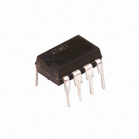
ATTINY13-20PJ Atmel, ATTINY13-20PJ Datasheet - Page 91

ATTINY13-20PJ
Manufacturer Part Number
ATTINY13-20PJ
Description
IC MCU AVR 1K 5V 20MHZ 8DIP
Manufacturer
Atmel
Series
AVR® ATtinyr
Specifications of ATTINY13-20PJ
Core Processor
AVR
Core Size
8-Bit
Speed
20MHz
Peripherals
Brown-out Detect/Reset, POR, PWM, WDT
Number Of I /o
6
Program Memory Size
1KB (512 x 16)
Program Memory Type
FLASH
Eeprom Size
64 x 8
Ram Size
64 x 8
Voltage - Supply (vcc/vdd)
2.7 V ~ 5.5 V
Data Converters
A/D 4x10b
Oscillator Type
Internal
Operating Temperature
-40°C ~ 85°C
Package / Case
8-DIP (0.300", 7.62mm)
Lead Free Status / RoHS Status
Lead free / RoHS Compliant
Connectivity
-
Other names
ATTINY13-24PJ
ATTINY13-24PJ
ATTINY13-24PJ
- Current page: 91 of 176
- Download datasheet (3Mb)
14.11 ADC Conversion Result
14.12 Register Description
14.12.1
2535J–AVR–08/10
ADMUX – ADC Multiplexer Selection Register
After the conversion is complete (ADIF is high), the conversion result can be found in the ADC
Result Registers (ADCL, ADCH).
For single ended conversion, the result is
where V
Table 14-2 on page 91
0x3FF represents the selected reference voltage minus one LSB.
• Bit 7 – Res: Reserved Bit
This bit is reserved bit in the ATtiny13 and will always read as zero.
• Bit 6 – REFS0: Reference Selection Bit
This bit selects the voltage reference for the ADC, as shown in
during a conversion, the change will not go in effect until this conversion is complete (ADIF in
ADCSRA is set).
Table 14-2.
• Bit 5 – ADLAR: ADC Left Adjust Result
The ADLAR bit affects the presentation of the ADC conversion result in the ADC Data Register.
Write one to ADLAR to left adjust the result. Otherwise, the result is right adjusted. Changing the
ADLAR bit will affect the ADC Data Register immediately, regardless of any ongoing conver-
sions. For a complete description of this bit, see
page
Bit
Read/Write
Initial Value
• Quantization Error: Due to the quantization of the input voltage into a finite number of codes,
• Absolute Accuracy: The maximum deviation of an actual (unadjusted) transition compared to
a range of input voltages (1 LSB wide) will code to the same value. Always ± 0.5 LSB.
an ideal transition for any code. This is the compound effect of offset, gain error, differential
error, non-linearity, and quantization error. Ideal value: ± 0.5 LSB.
93.
IN
is the voltage on the selected input pin and V
REFS0
Voltage Reference Selections for ADC
0
1
R
7
–
0
REFS0
and
R/W
6
0
Table 14-3 on page
ADLAR
Voltage Reference Selection
V
Internal Voltage Reference.
R/W
CC
5
0
used as analog reference.
ADC
=
R
4
–
0
V
--------------------------
IN
“ADCL and ADCH – The ADC Data Register” on
V
⋅
REF
1024
92). 0x000 represents analog ground, and
R
3
–
0
REF
the selected voltage reference (see
R
2
–
0
Table
MUX1
14-2. If this bit is changed
R/W
1
0
MUX0
R/W
0
0
ADMUX
91
Related parts for ATTINY13-20PJ
Image
Part Number
Description
Manufacturer
Datasheet
Request
R

Part Number:
Description:
IC MCU AVR 1K FLASH 20MHZ 8SOIC
Manufacturer:
Atmel
Datasheet:

Part Number:
Description:
Manufacturer:
Atmel Corporation
Datasheet:

Part Number:
Description:
IC MCU AVR 1K FLASH 20MHZ 8SOIC
Manufacturer:
Atmel
Datasheet:

Part Number:
Description:
IC MCU AVR 1K FLASH 10MHZ 20-MLF
Manufacturer:
Atmel
Datasheet:

Part Number:
Description:
IC MCU AVR 1K FLASH 20MHZ 8DIP
Manufacturer:
Atmel
Datasheet:

Part Number:
Description:
MCU AVR 1KB FLASH 20MHZ 3X3 QFN
Manufacturer:
Atmel
Datasheet:

Part Number:
Description:
IC MCU AVR 1K FLASH 20MHZ 8SOIC
Manufacturer:
Atmel
Datasheet:

Part Number:
Description:
IC MCU AVR 1K 5V 20MHZ 8SOIC
Manufacturer:
Atmel
Datasheet:

Part Number:
Description:
IC MCU AVR 1K 5V 20MHZ 8SOIC
Manufacturer:
Atmel
Datasheet:

Part Number:
Description:
IC MCU AVR 1K FLASH 20MHZ 8DIP
Manufacturer:
Atmel
Datasheet:

Part Number:
Description:
IC MCU AVR 1K FLASH 20MHZ 8SOIC
Manufacturer:
Atmel
Datasheet:

Part Number:
Description:
MCU AVR 1KB FLASH 20MHZ 8SOIC GW
Manufacturer:
Atmel
Datasheet:


