ATTINY13-20PJ Atmel, ATTINY13-20PJ Datasheet - Page 32
ATTINY13-20PJ
Manufacturer Part Number
ATTINY13-20PJ
Description
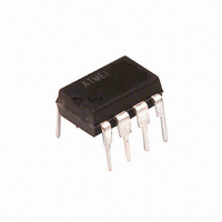
IC MCU AVR 1K 5V 20MHZ 8DIP
Manufacturer
Atmel
Series
AVR® ATtinyr
Specifications of ATTINY13-20PJ
Core Processor
AVR
Core Size
8-Bit
Speed
20MHz
Peripherals
Brown-out Detect/Reset, POR, PWM, WDT
Number Of I /o
6
Program Memory Size
1KB (512 x 16)
Program Memory Type
FLASH
Eeprom Size
64 x 8
Ram Size
64 x 8
Voltage - Supply (vcc/vdd)
2.7 V ~ 5.5 V
Data Converters
A/D 4x10b
Oscillator Type
Internal
Operating Temperature
-40°C ~ 85°C
Package / Case
8-DIP (0.300", 7.62mm)
Lead Free Status / RoHS Status
Lead free / RoHS Compliant
Connectivity
-
Other names
ATTINY13-24PJ
ATTINY13-24PJ
ATTINY13-24PJ


7.2.4
7.2.5
7.2.6
7.3
7.3.1
32
Register Description
ATtiny13
Internal Voltage Reference
Watchdog Timer
Port Pins
MCUCR – MCU Control Register
The Internal Voltage Reference will be enabled when needed by the Brown-out Detection, the
Analog Comparator or the ADC. If these modules are disabled as described in the sections
above, the internal voltage reference will be disabled and it will not be consuming power. When
turned on again, the user must allow the reference to start up before the output is used. If the
reference is kept on in sleep mode, the output can be used immediately. Refer to
age Reference” on page 37
If the Watchdog Timer is not needed in the application, this module should be turned off. If the
Watchdog Timer is enabled, it will be enabled in all sleep modes, and hence, always consume
power. In the deeper sleep modes, this will contribute significantly to the total current consump-
tion. Refer to
When entering a sleep mode, all port pins should be configured to use minimum power. The
most important thing is then to ensure that no pins drive resistive loads. In sleep modes where
both the I/O clock (clk
will be disabled. This ensures that no power is consumed by the input logic when not needed. In
some cases, the input logic is needed for detecting wake-up conditions, and it will then be
enabled. Refer to the section
which pins are enabled. If the input buffer is enabled and the input signal is left floating or has an
analog signal level close to V
For analog input pins, the digital input buffer should be disabled at all times. An analog signal
level close to V
input buffers can be disabled by writing to the Digital Input Disable Register (DIDR0). Refer to
“DIDR0 – Digital Input Disable Register 0” on page 80
The MCU Control Register contains control bits for power management.
• Bit 5 – SE: Sleep Enable
The SE bit must be written to logic one to make the MCU enter the sleep mode when the SLEEP
instruction is executed. To avoid the MCU entering the sleep mode unless it is the programmer’s
purpose, it is recommended to write the Sleep Enable (SE) bit to one just before the execution of
the SLEEP instruction and to clear it immediately after waking up.
Bit
Read/Write
Initial Value
“Interrupts” on page 44
CC
R
7
–
0
/2 on an input pin can cause significant current even in active mode. Digital
I/O
) and the ADC clock (clk
PUD
R/W
6
0
for details on the start-up time.
CC
“Digital Input Enable and Sleep Modes” on page 52
/2, the input buffer will use excessive power.
R/W
SE
5
0
for details on how to configure the Watchdog Timer.
SM1
R/W
4
0
ADC
) are stopped, the input buffers of the device
SM0
R/W
3
0
for details.
—
R
2
0
ISC01
R/W
1
0
ISC00
R/W
0
0
“Internal Volt-
2535J–AVR–08/10
for details on
MCUCR
Related parts for ATTINY13-20PJ
Image
Part Number
Description
Manufacturer
Datasheet
Request
R

Part Number:
Description:
IC MCU AVR 1K FLASH 20MHZ 8SOIC
Manufacturer:
Atmel
Datasheet:

Part Number:
Description:
Manufacturer:
Atmel Corporation
Datasheet:
Part Number:
Description:
IC MCU AVR 1K FLASH 20MHZ 8SOIC
Manufacturer:
Atmel
Datasheet:

Part Number:
Description:
IC MCU AVR 1K FLASH 10MHZ 20-MLF
Manufacturer:
Atmel
Datasheet:

Part Number:
Description:
IC MCU AVR 1K FLASH 20MHZ 8DIP
Manufacturer:
Atmel
Datasheet:

Part Number:
Description:
MCU AVR 1KB FLASH 20MHZ 3X3 QFN
Manufacturer:
Atmel
Datasheet:
Part Number:
Description:
IC MCU AVR 1K FLASH 20MHZ 8SOIC
Manufacturer:
Atmel
Datasheet:
Part Number:
Description:
IC MCU AVR 1K 5V 20MHZ 8SOIC
Manufacturer:
Atmel
Datasheet:
Part Number:
Description:
IC MCU AVR 1K 5V 20MHZ 8SOIC
Manufacturer:
Atmel
Datasheet:
Part Number:
Description:
IC MCU AVR 1K FLASH 20MHZ 8DIP
Manufacturer:
Atmel
Datasheet:
Part Number:
Description:
IC MCU AVR 1K FLASH 20MHZ 8SOIC
Manufacturer:
Atmel
Datasheet:
Part Number:
Description:
MCU AVR 1KB FLASH 20MHZ 8SOIC GW
Manufacturer:
Atmel
Datasheet: