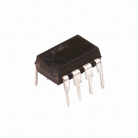
ATTINY15L-1PI Atmel, ATTINY15L-1PI Datasheet - Page 57

ATTINY15L-1PI
Manufacturer Part Number
ATTINY15L-1PI
Description
IC AVR MCU 1K FLASH 2.7V 8DIP
Manufacturer
Atmel
Series
AVR® ATtinyr
Specifications of ATTINY15L-1PI
Core Processor
AVR
Core Size
8-Bit
Speed
1.6MHz
Peripherals
Brown-out Detect/Reset, POR, PWM, WDT
Number Of I /o
6
Program Memory Size
1KB (512 x 16)
Program Memory Type
FLASH
Eeprom Size
64 x 8
Voltage - Supply (vcc/vdd)
2.7 V ~ 5.5 V
Data Converters
A/D 4x10b
Oscillator Type
Internal
Operating Temperature
-40°C ~ 85°C
Package / Case
8-DIP (0.300", 7.62mm)
Lead Free Status / RoHS Status
Contains lead / RoHS non-compliant
Ram Size
-
Connectivity
-
Available stocks
Company
Part Number
Manufacturer
Quantity
Price
Company:
Part Number:
ATTINY15L-1PI
Manufacturer:
AIMEL
Quantity:
5 510
Company:
Part Number:
ATTINY15L-1PI
Manufacturer:
VISHAY
Quantity:
5 510
Part Number:
ATTINY15L-1PI
Manufacturer:
ATMEL/爱特梅尔
Quantity:
20 000
Table 25. High-voltage Serial Programming Instruction Set for ATtiny15L
1187H–AVR–09/07
Instruction
Chip Erase
Write Flash
High and Low
Address
Write Flash
Low Byte
Write Flash
High Byte
Read Flash
High and Low
Address
Read Flash
Low Byte
Read Flash
High Byte
Write
EEPROM
Low Address
Write
EEPROM
Byte
Read
EEPROM
Low Address
Read
EEPROM
Byte
Write Fuse
Bits
Write Lock
Bits
Read Fuse
Bits
PB0
PB1
PB2
PB0
PB1
PB2
PB0
PB1
PB2
PB0
PB1
PB2
PB0
PB1
PB2
PB0
PB1
PB2
PB0
PB1
PB2
PB0
PB1
PB2
PB0
PB1
PB2
PB0
PB1
PB2
PB0
PB1
PB2
PB0
PB1
PB2
PB0
PB1
PB2
PB0
PB1
PB2
0_1000_0000_00
0_0100_1100_00
0_0001_0000_00
0_0100_1100_00
0_ i i i i_i i i i _00
0_0010_1100_00
0_ i i i i_i i i i _00
0_0000_0000_00
0_0110_1000_00
0_0000_0000_00
0_0111_1000_00
0_0001_0001_00
0_0100_1100_00
0_ i i i i_i i i i _00
0_0010_1100_00
0_0000_0011_00
0_0100_1100_00
0_0100_0000_00
0_0100_1100_00
0_0010_0000_00
0_0100_1100_00
0_0000_0100_00
0_0100_1100_00
0_0011_1100_00
0_0000_0010_00
0_0100_1100_00
0_0000_0000_00
0_0110_1000_00
x_xxxx_xxxx_xx
x_xxxx_xxxx_xx
x_xxxx_xxxx_xx
x_xxxx_xxxx_xx
x_xxxx_xxxx_xx
x_xxxx_xxxx_xx
x_xxxx_xxxx_xx
x_xxxx_xxxx_xx
x_xxxx_xxxx_xx
x_xxxx_xxxx_xx
x_xxxx_xxxx_xx
x_xxxx_xxxx_xx
x_xxxx_xxxx_xx
x_xxxx_xxxx_xx
Instr.1
0_00bb_bbbb_00
0_00bb_bbbb_00
o_oooo_ooox_xx
o_oooo_ooox_xx
o_oooo_ooox_xx
0_0000_0000_00
0_0110_0100_00
0_0000_000a_00
0_0001_1100_00
0_0000_0000_00
0_0110_0100_00
0_0000_0000_00
0_0111_0100_00
0_0000_000a_00
0_0001_1100_00
0_0000_0000_00
0_0110_1100_00
0_0000_0000_00
0_0110_1100_00
0_0000_1100_00
0_0000_0000_00
0_0110_0100_00
0_0000_1100_00
0_0000_0000_00
0_0110_1100_00
0_8765_1143_00
0_0010_1100_00
0_0000_0210_00
0_0010_1100_00
0_0000_0000_00
0_0110_1000_00
x_xxxx_xxxx_xx
x_xxxx_xxxx_xx
x_xxxx_xxxx_xx
x_xxxx_xxxx_xx
x_xxxx_xxxx_xx
x_xxxx_xxxx_xx
x_xxxx_xxxx_xx
x_xxxx_xxxx_xx
x_xxxx_xxxx_xx
x_xxxx_xxxx_xx
x_xxxx_xxxx_xx
Instr.2
Instruction Format
0_bbbb_bbbb_00
0_bbbb_bbbb_00
0_0000_0000_00
0_0110_1100_00
0_0000_1100_00
0_0000_0000_00
0_0110_1100_00
0_0000_0000_00
0_0000_0000_00
0_0111_1100_00
0_0000_0000_00
0_0000_1100_00
0_0000_0000_00
0_0110_1100_00
0_0000_0000_00
0_0000_0000_00
0_0110_0100_00
0_0000_0000_00
0_0110_0100_00
0_0000_0000_00
0_0110_1100_00
8_765x_x43x_xx
x_xxxx_xxxx_xx
x_xxxx_xxxx_xx
x_xxxx_xxxx_xx
x_xxxx_xxxx_xx
x_xxxx_xxxx_xx
Instr.3
(1)
0_0000_0000_00
0_0100_1100_00
0_0000_0000_00
0_0110_1100_00
0_0000_0000_00
0_0110_1100_00
0_0000_0000_00
x_xxxx_xxxx_xx
x_xxxx_xxxx_xx
Instr.4
Operation Remarks
Wait after Instr.3 until PB2
goes high for the Chip Erase
cycle to finish.
Repeat Instr.2 for a new 256
byte page. Repeat Instr.3 for
each new address.
Wait after Instr.3 until PB2
goes high. Repeat Instr.1,
Instr. 2 and Instr.3 for each
new address.
Wait after Instr.3 until PB2
goes high. Repeat Instr.1,
Instr. 2 and Instr.3 for each
new address.
Repeat Instr.2 and Instr.3 for
each new address.
Repeat Instr.1 and Instr.2 for
each new address.
Repeat Instr.1 and Instr.2 for
each new address.
Repeat Instr.2 for each new
address.
Wait after Instr.3 until PB2
goes high
Repeat Instr.2 for each new
address.
Repeat Instr.2 for each new
address
Wait after Instr.4 until PB2
goes high. Write 8 - 3 = “0” to
program the Fuse bit.
Wait after Instr.4 until PB2
goes high. Write 2, 1 = “0” to
program the Lock bit.
Reading 8 - 3 = “0” means the
Fuse bit is programmed.
ATtiny15L
57


