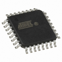
AT90LS2333-4AI Atmel, AT90LS2333-4AI Datasheet - Page 33

AT90LS2333-4AI
Manufacturer Part Number
AT90LS2333-4AI
Description
IC MCU 2K 4MHZ A/D LV IT 32TQFP
Manufacturer
Atmel
Series
AVR® 90LSr
Datasheet
1.AT90LS2333-4AC.pdf
(103 pages)
Specifications of AT90LS2333-4AI
Core Processor
AVR
Core Size
8-Bit
Speed
4MHz
Connectivity
SPI, UART/USART
Peripherals
Brown-out Detect/Reset, POR, PWM, WDT
Number Of I /o
20
Program Memory Size
2KB (1K x 16)
Program Memory Type
FLASH
Eeprom Size
128 x 8
Ram Size
128 x 8
Voltage - Supply (vcc/vdd)
2.7 V ~ 6 V
Data Converters
A/D 6x10b
Oscillator Type
Internal
Operating Temperature
-40°C ~ 85°C
Package / Case
32-TQFP, 32-VQFP
Lead Free Status / RoHS Status
Contains lead / RoHS non-compliant
Table 12. Clock 1 Prescale Select
The Stop condition provides a Timer Enable/Disable function. The prescaled CK modes are scaled directly from the CK
oscillator clock. If the external pin modes are used for Timer/Counter0, transitions on PD5/(T1) will clock the counter even if
the pin is configured as an output. This feature can give the user SW control of the counting.
Timer/Counter1 - TCNT1H and TCNT1L
This 16-bit register contains the prescaled value of the 16-bit Timer/Counter1. To ensure that both the high and low bytes
are read and written simultaneously when the CPU accesses these registers, the access is performed using an 8-bit tem-
porary register (TEMP). This temporary register is also used when accessing OCR1 and ICR1. If the main program and
also interrupt routines perform access to registers using TEMP, interrupts must be disabled during access from the main
program (and from interrupt routines if interrupts are allowed from within interrupt routines).
•
When the CPU writes to the high byte TCNT1H, the written data is placed in the TEMP register. Next, when the CPU writes
the low byte TCNT1L, this byte of data is combined with the byte data in the TEMP register, and all 16 bits are written to the
TCNT1 Timer/Counter1 register simultaneously. Consequently, the high byte TCNT1H must be accessed first for a full 16-
bit register write operation.
•
When the CPU reads the low byte TCNT1L, the data of the low byte TCNT1L is sent to the CPU and the data of the high
byte TCNT1H is placed in the TEMP register. When the CPU reads the data in the high byte TCNT1H, the CPU receives
the data in the TEMP register. Consequently, the low byte TCNT1L must be accessed first for a full 16-bit register read
operation.
The Timer/Counter1 is realized as an up or up/down (in PWM mode) counter with read and write access. If Timer/Counter1
is written to and a clock source is selected, the Timer/Counter1 continues counting in the timer clock cycle after it is preset
with the written value.
Bit
$2D ($4D)
$2C ($4C)
Read/Write
Initial value
TCNT1 Timer/Counter1 Write
TCNT1 Timer/Counter1 Read
CS12
0
0
0
0
1
1
1
1
CS11
MSB
R/W
R/W
15
7
0
0
0
0
1
1
0
0
1
1
R/W
R/W
14
6
0
0
CS10
0
1
0
1
0
1
0
1
R/W
R/W
13
5
0
0
Description
Stop, the Timer/Counter1 is stopped.
CK
CK / 8
CK / 64
CK / 256
CK / 1024
External Pin T1, falling edge
External Pin T1, rising edge
R/W
R/W
12
4
0
0
AT90S/LS2333 and AT90S/LS4433
R/W
R/W
11
3
0
0
R/W
R/W
10
2
0
0
R/W
R/W
9
1
0
0
LSB
R/W
R/W
8
0
0
0
TCNT1H
TCNT1L
33


