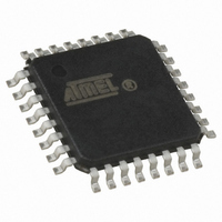
AT90LS2333-4AI Atmel, AT90LS2333-4AI Datasheet - Page 31

AT90LS2333-4AI
Manufacturer Part Number
AT90LS2333-4AI
Description
IC MCU 2K 4MHZ A/D LV IT 32TQFP
Manufacturer
Atmel
Series
AVR® 90LSr
Datasheet
1.AT90LS2333-4AC.pdf
(103 pages)
Specifications of AT90LS2333-4AI
Core Processor
AVR
Core Size
8-Bit
Speed
4MHz
Connectivity
SPI, UART/USART
Peripherals
Brown-out Detect/Reset, POR, PWM, WDT
Number Of I /o
20
Program Memory Size
2KB (1K x 16)
Program Memory Type
FLASH
Eeprom Size
128 x 8
Ram Size
128 x 8
Voltage - Supply (vcc/vdd)
2.7 V ~ 6 V
Data Converters
A/D 6x10b
Oscillator Type
Internal
Operating Temperature
-40°C ~ 85°C
Package / Case
32-TQFP, 32-VQFP
Lead Free Status / RoHS Status
Contains lead / RoHS non-compliant
When Timer/Counter1 is externally clocked, the external signal is synchronized with the oscillator frequency of the CPU. To
assure proper sampling of the external clock, the minimum time between two external clock transitions must be at least one
internal CPU clock period. The external clock signal is sampled on the rising edge of the internal CPU clock.
The 16-bit Timer/Counter1 features both a high resolution and a high accuracy usage with the lower prescaling opportuni-
ties. Similarly, the high prescaling opportunities makes the Timer/Counter1 useful for lower speed functions or exact timing
functions with infrequent actions.
The Timer/Counter1 supports an Output Compare function using the Output Compare Register 1 - OCR1 as the data
source to be compared to the Timer/Counter1 contents. The Output Compare functions include optional clearing of the
counter on compare matches, and actions on the Output Compare pin 1 on compare matches.
Timer/Counter1 can also be used as a 8, 9 or 10-bit Pulse With Modulator. In this mode the counter and the OCR1 register
serve as a glitch-free stand-alone PWM with centered pulses. Refer to page 34 for a detailed description on this function.
The Input Capture function of Timer/Counter1 provides a capture of the Timer/Counter1 contents to the Input Capture Reg-
ister - ICR1, triggered by an external event on the Input Capture Pin - ICP. The actual capture event settings are defined by
the Timer/Counter1 Control Register - TCCR1. In addition, the Analog Comparator can be set to trigger the Input Capture.
Refer to the section, “The Analog Comparator”, for details on this. The ICP pin logic is shown in Figure 33.
Figure 33. ICP Pin Schematic Diagram
If the noise canceler function is enabled, the actual trigger condition for the capture event is monitored over 4 samples, and
all 4 must be equal to activate the capture flag. The input pin signal is sampled at XTAL clock frequency.
Timer/Counter1 Control Register A - TCCR1A
•
The COM11 and COM10 control bits determine any output pin action following a compare match in Timer/Counter1. Any
output pin actions affect pin OC1 - Output Compare pin 1. This is an alternative function to an I/O port, and the correspond-
ing direction control bit must be set (one) to control an output pin. The control configuration is shown in Table 10.
Table 10. Compare 1 Mode Select
In PWM mode, these bits have a different function. Refer to Table 11 for a detailed description.
Bit
$2F ($4F)
Read/Write
Initial value
Bits 7,6 - COM11, COM10: Compare Output Mode1, bits 1 and 0
COM11
0
0
1
1
COM11
R/W
7
0
COM10
0
1
0
1
COM10
R/W
6
0
Timer/Counter1 disconnected from output pin OC1
Toggle the OC1 output line.
Clear the OC1 output line (to zero).
Set the OC1 output line (to one).
Description
R
5
0
-
R
4
0
-
AT90S/LS2333 and AT90S/LS4433
R
3
0
-
R
2
0
-
PWM11
R/W
1
0
PWM10
R/W
0
0
TCCR1A
31


