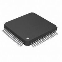
MAXQ622G-0000+ Maxim Integrated Products, MAXQ622G-0000+ Datasheet - Page 10

MAXQ622G-0000+
Manufacturer Part Number
MAXQ622G-0000+
Description
IC MCU 16BIT 64K IR MOD 64LQFP
Manufacturer
Maxim Integrated Products
Series
MAXQ™r
Datasheet
1.MAXQ622G-0000.pdf
(31 pages)
Specifications of MAXQ622G-0000+
Core Processor
RISC
Core Size
16-Bit
Speed
12MHz
Connectivity
I²C, SPI, UART/USART, USB
Peripherals
Brown-out Detect/Reset, Infrared, Power-Fail, POR, WDT
Number Of I /o
44
Program Memory Size
128KB (128K x 8)
Program Memory Type
FLASH
Ram Size
6K x 8
Voltage - Supply (vcc/vdd)
1.7 V ~ 3.6 V
Oscillator Type
Internal
Operating Temperature
0°C ~ 70°C
Package / Case
64-LQFP
Processor Series
MAXQ622
Core
RISC
Data Bus Width
16 bit
Data Ram Size
6 KB
Interface Type
I2C, SPI, USART
Maximum Clock Frequency
12 MHz
Number Of Programmable I/os
44
Number Of Timers
2
Operating Supply Voltage
1.7 V to 3.6 V
Maximum Operating Temperature
+ 70 C
Mounting Style
SMD/SMT
Development Tools By Supplier
MAXQUSBJTAG-KIT MAXQ622-KIT
Minimum Operating Temperature
0 C
For Use With
MAXQ622-KIT# - EVALUATION KIT FOR MAXQ622
Lead Free Status / RoHS Status
Lead free / RoHS Compliant
Eeprom Size
-
Data Converters
-
Lead Free Status / Rohs Status
Details
Note 15: For USB operation, both V
Note 16: FRCVDD is the force V
Note 17: The ESD protection scheme is in production on existing parts. The 1FF capacitor on V
Note 18: Devices that use nonstandard supply voltages that do not conform to the intended I
Note 19: The maximum fall time, t
Note 20: C
Note 21: All values referred to V
Note 22: A device must internally provide a hold time of at least 300ns for the SDA signal (referred to the V
Note 23: The maximum t
Note 24: A fast-mode I
Note 25: AC electrical specifications are guaranteed by design and are not production tested.
Figure 1. Series Resistors (R
Figure 2. I
16-Bit Microcontrollers with
Infrared Module and Optional USB
10
SDA
SCL
NOTE: TIMING REFERENCED TO V
_____________________________________________________________________________________
is always used as the core 3V power supply.
pin from ESD damage (rather than DP or DM) since it is externally exposed. The ESD test uses 150pF charged to 15kV
applied to the 1FF capacitor creating a delta V of approximately 2.25V and limiting the voltage on V
input levels to the voltage to which the pullup resistors R
250ns for the output stages. This allows series protection resistors (R
the SDA/SCL bus lines as shown in I
signal) to bridge the undefined region of the falling edge of SCL.
be met. This is automatically the case if the device does not stretch the low period of the SCL signal. If such a device
does stretch the low period of the SCL signal, it must output the next data bit to the SDA line t
1000 + 250 = 1250ns (according to the standard-mode I
2
B
C Bus Controller Timing Diagram
t
F_I2C
= Capacitance of one bus line in pF.
S
2
t
C bus device can be used in a standard-mode I
LOW_I2C
t
HD:STA
HD:DAT
IH_I2C(MIN)
S
) for Protecting Against High-Voltage Spikes
DD
IH_I2C(MIN)
need only be met if the device does not stretch the low period (t
F_I2C
AND V
DD
power-supply bit (PWCN.10). When FRCVDD = 1, V
t
HD:DAT
MAXQ612
MAXQ622
and V
IL_I2C(MAX).
of 300ns for the SDA and SCL bus lines is longer than the specificed maximum t
t
R_I2C
and V
P0.3
P0.4
BUS
2
C Bus Controller Timing without exceeding the maximum specified fall time.
SDA
SCL
must be connected.
IL_I2C (MAX)
t
SU:DAT
DEVICE
t
HIGH_I2C
I
R
2
C
S
.
R
S
P
2
C specification) before the SCL line is released.
are connected.
2
DEVICE
C bus system, but the requirement t
V
I
R
2
DD
C
S
S
SR
) to be connected between the SDA/SCL pins and
R
S
t
SU:STA
DDB
R
P
power switching is disabled, and V
2
C bus system levels must relate their
R
BUS
P
LOW_I2C
is intended to protect that
t
SU:STO
R_I2C(MAX)
) of the SCL signal.
IH_I2C(MIN)
BUS
SU:DAT
P
.
+ t
t
BUF
R 250ns must
SU:DAT
of the SCL
OF_I2C
S
=
DD
of


