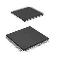
DF2168VTE33 Renesas Electronics America, DF2168VTE33 Datasheet - Page 681

DF2168VTE33
Manufacturer Part Number
DF2168VTE33
Description
MCU FLASH 3V 256K 33MHZ 144TQFP
Manufacturer
Renesas Electronics America
Series
H8® H8S/2100r
Datasheet
1.HS2168EPI61H-U.pdf
(876 pages)
Specifications of DF2168VTE33
Core Processor
H8S/2000
Core Size
16-Bit
Speed
33MHz
Connectivity
I²C, IrDA, LPC, SCI, SmartCard
Peripherals
POR, PWM, WDT
Number Of I /o
106
Program Memory Size
256KB (256K x 8)
Program Memory Type
FLASH
Ram Size
40K x 8
Voltage - Supply (vcc/vdd)
3 V ~ 3.6 V
Data Converters
A/D 8x10b; D/A 2x8b
Oscillator Type
Internal
Operating Temperature
-20°C ~ 75°C
Package / Case
144-TQFP, 144-VQFP
Lead Free Status / RoHS Status
Contains lead / RoHS non-compliant
Eeprom Size
-
Available stocks
Company
Part Number
Manufacturer
Quantity
Price
Company:
Part Number:
DF2168VTE33WV
Manufacturer:
Renesas Electronics America
Quantity:
10 000
- Current page: 681 of 876
- Download datasheet (5Mb)
The system configuration diagram in boot mode is shown in figure 20.6. For details on the pin
setting in boot mode, see table 20.5. The NMI and other interrupts are ignored in boot mode.
However, the NMI and other interrupts should be disabled in the user system.
(1)
When boot mode is initiated, this LSI measures the low period of asynchronous SCI-communica-
tion data (H'00), which is transmitted consecutively by the host. The SCI transmit/receive format
is set to 8-bit data, 1 stop bit, and no parity. This LSI calculates the bit rate of transmission by the
host by means of the measured low period and transmits the bit adjustment end sign (1 byte of
H'00) to the host. The host must confirm that this bit adjustment end sign (H'00) has been received
normally and transmits 1 byte of H'55 to this LSI. When reception is not executed normally, boot
mode is initiated again (reset) and the operation described above must be executed. The bit rate
between the host and this LSI is not matched by the bit rate of transmission by the host and system
clock frequency of this LSI. To operate the SCI normally, the transfer bit rate of the host must be
set to 4,800 bps, 9,600 bps, or 19,200 bps.
The system clock frequency, which can automatically adjust the transfer bit rate of the host and
the bit rate of this LSI, is shown in table 20.6. Boot mode must be initiated in the range of this
system clock.
SCI Interface Setting by Host
tool and program
programming
Boot
Host
data
Start
bit
Figure 20.7 Automatic-Bit-Rate Adjustment Operation of SCI
D0
Figure 20.6 System Configuration in Boot Mode
Measure low period (9 bits) (data is H'00)
Control command, program data
D1
Reply response
D2
D3
D4
analysis execution
Control command,
software (on-chip)
RxD1
T xD1
On-chip SCI_1
D5
D6
Rev. 3.00, 03/04, page 639 of 830
This LSI
D7
On-chip RAM
High period of
at least 1 bit
Stop bit
memory
Flash
Related parts for DF2168VTE33
Image
Part Number
Description
Manufacturer
Datasheet
Request
R

Part Number:
Description:
0.6mm Pitch Board-to-Fine-Coaxial Cable Connectors
Manufacturer:
Hirose Electric
Datasheet:

Part Number:
Description:
0.6mm Pitch Board-to-fine-coaxial Cable Connectors
Manufacturer:
Hirose Electric
Datasheet:

Part Number:
Description:
0.6mm Pitch Board-to-fine-coaxial Cable Connectors
Manufacturer:
Hirose Electric
Datasheet:

Part Number:
Description:
Right angle, Two-piece for fine coaxial cable, Discrete wire connectors; HRS No: 687-0001-5 56; No. of Positions: 20; Connector Type: Board mounting; Contact Gender: Female; Contact Spacing (mm): 0.6; Terminal Pitch (mm): 0.6; PCB Mount Type: SMT; Cu
Manufacturer:
Hirose Electric

Part Number:
Description:
0.6mm Pitch Board-to-fine-coaxial Cable Connectors
Manufacturer:
Hirose Electric
Datasheet:

Part Number:
Description:
0.6mm Pitch Board-to-Fine-Coaxial Cable Connectors
Manufacturer:
HIROSE [Hirose Electric]
Datasheet:

Part Number:
Description:
KIT STARTER FOR M16C/29
Manufacturer:
Renesas Electronics America
Datasheet:

Part Number:
Description:
KIT STARTER FOR R8C/2D
Manufacturer:
Renesas Electronics America
Datasheet:

Part Number:
Description:
R0K33062P STARTER KIT
Manufacturer:
Renesas Electronics America
Datasheet:

Part Number:
Description:
KIT STARTER FOR R8C/23 E8A
Manufacturer:
Renesas Electronics America
Datasheet:

Part Number:
Description:
KIT STARTER FOR R8C/25
Manufacturer:
Renesas Electronics America
Datasheet:

Part Number:
Description:
KIT STARTER H8S2456 SHARPE DSPLY
Manufacturer:
Renesas Electronics America
Datasheet:

Part Number:
Description:
KIT STARTER FOR R8C38C
Manufacturer:
Renesas Electronics America
Datasheet:

Part Number:
Description:
KIT STARTER FOR R8C35C
Manufacturer:
Renesas Electronics America
Datasheet:

Part Number:
Description:
KIT STARTER FOR R8CL3AC+LCD APPS
Manufacturer:
Renesas Electronics America
Datasheet:


