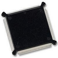
MC68HC16Z1CEH25 Freescale Semiconductor, MC68HC16Z1CEH25 Datasheet - Page 257

MC68HC16Z1CEH25
Manufacturer Part Number
MC68HC16Z1CEH25
Description
IC MCU 16BIT 25MHZ 132-PQFP
Manufacturer
Freescale Semiconductor
Series
HC16r
Datasheet
1.MC68HC16Z1VEH16.pdf
(500 pages)
Specifications of MC68HC16Z1CEH25
Core Processor
CPU16
Core Size
16-Bit
Speed
25MHz
Connectivity
EBI/EMI, SCI, SPI
Peripherals
POR, PWM, WDT
Number Of I /o
16
Program Memory Type
ROMless
Ram Size
1K x 8
Voltage - Supply (vcc/vdd)
2.7 V ~ 5.5 V
Data Converters
A/D 8x10b
Oscillator Type
Internal
Operating Temperature
-40°C ~ 85°C
Package / Case
132-QFP
Package
132PQFP
Family Name
HC16
Maximum Speed
25 MHz
Operating Supply Voltage
3.3|5 V
Data Bus Width
16 Bit
Number Of Programmable I/os
16
On-chip Adc
8-chx10-bit
Number Of Timers
11
Controller Family/series
68HC16
No. Of I/o's
16
Ram Memory Size
1KB
Cpu Speed
25MHz
No. Of Timers
2
Embedded Interface Type
QSPI, SCI
Rohs Compliant
Yes
Processor Series
HC16Z
Core
CPU16
Data Ram Size
1 KB
Interface Type
SCI, SPI, UART
Maximum Clock Frequency
25 MHz
Maximum Operating Temperature
+ 85 C
Mounting Style
SMD/SMT
Minimum Operating Temperature
- 40 C
Lead Free Status / RoHS Status
Lead free / RoHS Compliant
Eeprom Size
-
Program Memory Size
-
Lead Free Status / Rohs Status
Details
Available stocks
Company
Part Number
Manufacturer
Quantity
Price
Company:
Part Number:
MC68HC16Z1CEH25
Manufacturer:
Freescale Semiconductor
Quantity:
135
Company:
Part Number:
MC68HC16Z1CEH25
Manufacturer:
Freescale Semiconductor
Quantity:
10 000
- Current page: 257 of 500
- Download datasheet (6Mb)
10.4.3 Receive Data Pins (RXDA, RXDB)
10.4.4 Transmit Data Pins (TXDA, TXDB)
10.4.5 SCI Operation
10.4.5.1 Definition of Terms
M68HC16 Z SERIES
USER’S MANUAL
RXDA and RXDB are the serial data inputs to the SCIA and SCIB interfaces, respec-
tively. Each pin is also available as a general-purpose I/O pin when the RE bit in
SCCR1 of the associated SCI submodule is cleared. When used for general-purpose
I/O, RXDA and RXDB may be configured either as input or output as determined by
the RXDA and RXDB bits in the MDDR.
When used for general-purpose I/O, TXDA and TXDB can be configured either as in-
put or output as determined by the TXDA and TXDB bits in the MDDR. The TXDA and
TXDB pins are enabled for SCI use by setting the TE bit in SCCR1 of each SCI inter-
face.
SCI operation can be polled by means of status flags in the SCSR, or interrupt-driven
operation can be employed by means of the interrupt-enable bits in SCCR1.
Data can be transmitted and received in a number of formats. The following terms con-
cerning data format are used in this section:
• Bit-Time — The time required to transmit or receive one bit of data, which is equal
• Start Bit — One bit-time of logic zero that indicates the beginning of a data frame.
• Stop Bit — One bit-time of logic one that indicates the end of a data frame.
• Frame — A complete unit of serial information. The SCI can use 10-bit or 11-bit
• Data Frame — A start bit, a specified number of data or information bits, and at
• Idle Frame — A frame that consists of consecutive ones. An idle frame has no
• Break Frame — A frame that consists of consecutive zeros. A break frame has
to one cycle of the baud frequency.
A start bit must begin with a one-to-zero transition and be preceded by at least
three receive time samples of logic one.
frames.
least one stop bit.
start bit.
no stop bits.
Transmit data
Receive data
Pin
MULTICHANNEL COMMUNICATION INTERFACE
Freescale Semiconductor, Inc.
TXDA
TXDB
RXDA
RXDB
Mode
For More Information On This Product,
Go to: www.freescale.com
Table 10-5 SCI Pins
Serial data output from SCIA (TE = 1)
Serial data output from SCIB (TE = 1)
Serial data input to SCIA (RE = 1)
Serial data input to SCIB (RE = 1)
SCI Function
Port I/O Signal
PMC7
PMC5
PMC6
PMC4
10-17
Related parts for MC68HC16Z1CEH25
Image
Part Number
Description
Manufacturer
Datasheet
Request
R
Part Number:
Description:
Manufacturer:
Freescale Semiconductor, Inc
Datasheet:
Part Number:
Description:
Manufacturer:
Freescale Semiconductor, Inc
Datasheet:
Part Number:
Description:
Manufacturer:
Freescale Semiconductor, Inc
Datasheet:
Part Number:
Description:
Manufacturer:
Freescale Semiconductor, Inc
Datasheet:
Part Number:
Description:
Manufacturer:
Freescale Semiconductor, Inc
Datasheet:
Part Number:
Description:
Manufacturer:
Freescale Semiconductor, Inc
Datasheet:
Part Number:
Description:
Manufacturer:
Freescale Semiconductor, Inc
Datasheet:
Part Number:
Description:
Manufacturer:
Freescale Semiconductor, Inc
Datasheet:
Part Number:
Description:
Manufacturer:
Freescale Semiconductor, Inc
Datasheet:
Part Number:
Description:
Manufacturer:
Freescale Semiconductor, Inc
Datasheet:
Part Number:
Description:
Manufacturer:
Freescale Semiconductor, Inc
Datasheet:
Part Number:
Description:
Manufacturer:
Freescale Semiconductor, Inc
Datasheet:
Part Number:
Description:
Manufacturer:
Freescale Semiconductor, Inc
Datasheet:
Part Number:
Description:
Manufacturer:
Freescale Semiconductor, Inc
Datasheet:
Part Number:
Description:
Manufacturer:
Freescale Semiconductor, Inc
Datasheet:


